Datasheet 搜索 > FPGA芯片 > Microsemi(美高森美) > APA300-FGG144 数据手册 > APA300-FGG144 数据手册 1/10 页
 器件3D模型
¥ 692.812
APA300-FGG144 数据手册 - Microsemi(美高森美)
制造商:
Microsemi(美高森美)
分类:
FPGA芯片
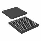
封装:
FBGA-144
Pictures:
3D模型
符号图
焊盘图
引脚图
产品图
页面导航:
导航目录
APA300-FGG144数据手册
Page:
of 10 Go
若手册格式错乱,请下载阅览PDF原文件
December 2009 i
© 2009 Actel Corporation See the Actel website for the latest version of the datasheet.
v5.9
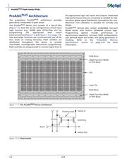
ProASIC
PLUS®
Flash Family FPGAs
Features and Benefits
High Capacity
Commercial and Industrial
• 75,000 to 1 Million System Gates
• 27 K to 198 Kbits of Two-Port SRAM
• 66 to 712 User I/Os
Military
• 300, 000 to 1 Million System Gates
• 72 K to 198 Kbits of Two Port SRAM
• 158 to 712 User I/Os
Reprogrammable Flash Technology
• 0.22 µm 4 LM Flash-Based CMOS Process
• Live At Power-Up (LAPU) Level 0 Support
• Single-Chip Solution
• No Configuration Device Required
• Retains Programmed Design during Power-Down/Up Cycles
• Mil/Aero Devices Operate over Full Military Temperature
Range
Performance
• 3.3 V, 32-Bit PCI, up to 50 MHz (33 MHz over military
temperature)
• Two Integrated PLLs
• External System Performance up to 150 MHz
Secure Programming
• The Industry’s Most Effective Security Key (FlashLock
®
)
Low Power
• Low Impedance Flash Switches
• Segmented Hierarchical Routing Structure
• Small, Efficient, Configurable (Combinatorial or Sequential)
Logic Cells
High Performance Routing Hierarchy
• Ultra-Fast Local and Long-Line Network
• High-Speed Very Long-Line Network
• High-Performance, Low Skew, Splittable Global Network
• 100% Routability and Utilization
I/O
• Schmitt-Trigger Option on Every Input
• 2.5 V / 3.3 V Support with Individually-Selectable Voltage
and Slew Rate
• Bidirectional Global I/Os
• Compliance with PCI Specification Revision 2.2
• Boundary-Scan Test IEEE Std. 1149.1 (JTAG) Compliant
• Pin-Compatible Packages across the ProASIC
PLUS
Family
Unique Clock Conditioning Circuitry
• PLL with Flexible Phase, Multiply/Divide, and Delay
Capabilities
• Internal and/or External Dynamic PLL Configuration
• Two LVPECL Differential Pairs for Clock or Data Inputs
Standard FPGA and ASIC Design Flow
• Flexibility with Choice of Industry-Standard Front-End Tools
• Efficient Design through Front-End Timing and Gate
Optimization
ISP Support
• In-System Programming (ISP) via JTAG Port
SRAMs and FIFOs
• SmartGen Netlist Generation Ensures Optimal Usage of
Embedded Memory Blocks
• 24 SRAM and FIFO Configurations with Synchronous and
Asynchronous Operation up to 150 MHz (typical)
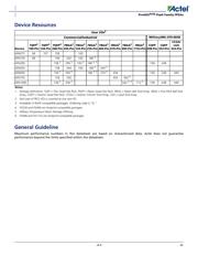
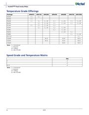
Table 1 • ProASIC
PLUS
Product Profile
Device APA075 APA150 APA300
1
APA450 APA600
1
APA750 APA1000
1
Maximum System Gates 75,000 150,000 300,000 450,000 600,000 750,000 1,000,000
Tiles (Registers) 3,072 6,144 8,192 12,288 21,504 32,768 56,320
Embedded RAM Bits (k=1,024 bits) 27 k 36k 72 k 108 k 126 k 144 k 198 k
Embedded RAM Blocks (256x9) 12 16 32 48 56 64 88
LVPECL 222 2 2 2 2
PLL 222 2 2 2 2
Global Networks 4 4 4 4 4 4 4
Maximum Clocks 24 32 32 48 56 64 88
Maximum User I/Os 158 242 290 344 454 562 712
JTAG ISP Yes Yes Yes Yes Yes Yes Yes
PCI Yes Yes Yes Yes Yes Yes Yes
Package (by pin count)
TQFP 100, 144 100 – – – – –
PQFP 208 208 208 208 208 208 208
PBGA – 456 456 456 456 456 456
FBGA 144 144, 256 144, 256 144, 256, 484 256, 484, 676 676, 896 896, 1152
CQFP
2
208, 352 208, 352 208, 352
CCGA/LGA
2
624 624
Notes:
1. Available as Commercial/Industrial and Military/MIL-STD-883B devices.
2. These packages are available only for Military/MIL-STD-883B devices.
v5.9
®
器件 Datasheet 文档搜索
AiEMA 数据库涵盖高达 72,405,303 个元件的数据手册,每天更新 5,000 多个 PDF 文件
