Datasheet 搜索 > Microchip(微芯) > AT28C64B-15JU-T 数据手册 > AT28C64B-15JU-T 数据手册 3/18 页
 器件3D模型
¥ 40.531
AT28C64B-15JU-T 数据手册 - Microchip(微芯)
制造商:
Microchip(微芯)
封装:
PLCC-32
描述:
EEPROM, 并行口, 64 Kbit, 8K x 8位, LCC, 32 引脚
Pictures:
3D模型
符号图
焊盘图
引脚图
产品图
页面导航:
导航目录
AT28C64B-15JU-T数据手册
Page:
of 18 Go
若手册格式错乱,请下载阅览PDF原文件
3
0270L–PEEPR–2/09
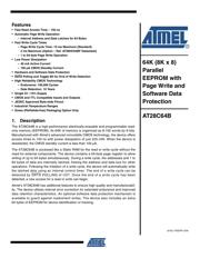
AT28C64B
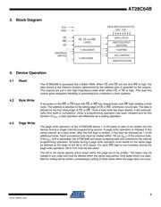
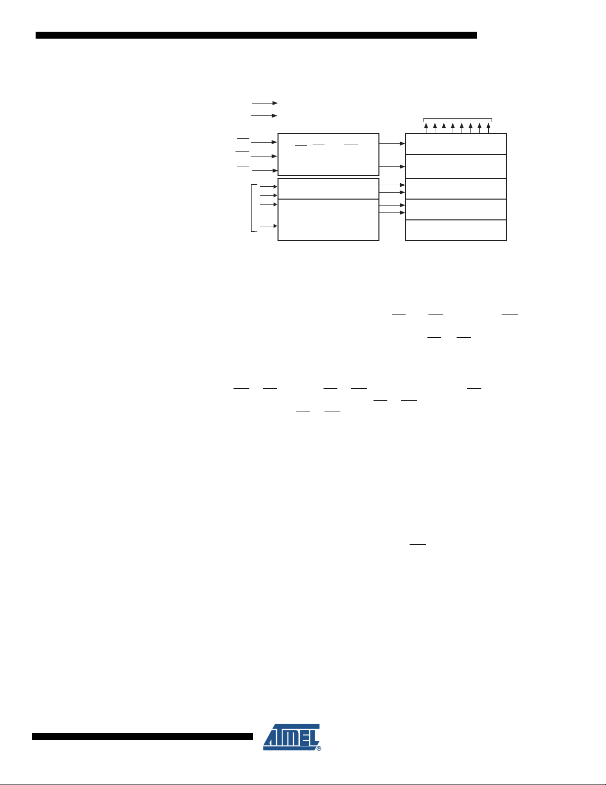
3. Block Diagram
4. Device Operation
4.1 Read
The AT28C64B is accessed like a Static RAM. When CE and OE are low and WE is high, the
data stored at the memory location determined by the address pins is asserted on the outputs.
The outputs are put in the high-impedance state when either CE
or OE is high. This dual line
control gives designers flexibility in preventing bus contention in their systems.
4.2 Byte Write
A low pulse on the WE or CE input with CE or WE low (respectively) and OE high initiates a write
cycle. The address is latched on the falling edge of CE
or WE, whichever occurs last. The data is
latched by the first rising edge of CE
or WE. Once a byte write has been started, it will automati-
cally time itself to completion. Once a programming operation has been initiated and for the
duration of t
WC
, a read operation will effectively be a polling operation.
4.3 Page Write
The page write operation of the AT28C64B allows 1 to 64 bytes of data to be written into the
device during a single internal programming period. A page write operation is initiated in the
same manner as a byte write; after the first byte is written, it can then be followed by 1 to 63
additional bytes. Each successive byte must be loaded within 150 µs (t
BLC
) of the previous byte.
If the t
BLC
limit is exceeded, the AT28C64B will cease accepting data and commence the internal
programming operation. All bytes during a page write operation must reside on the same page
as defined by the state of the A6 to A12 inputs. For each WE
high to low transition during the
page write operation, A6 to A12 must be the same.
The A0 to A5 inputs specify which bytes within the page are to be written. The bytes may be
loaded in any order and may be altered within the same load period. Only bytes which are spec-
ified for writing will be written; unnecessary cycling of other bytes within the page does not occur.
VCC
GND
OE
WE
CE
ADDRESS
INPUTS
X DECODER
Y DECODER
OE, CE and WE
LOGIC
DATA INPUTS/OUTPUTS
I/O0 - I/O7
DATA LATCH
INPUT/OUTPUT
BUFFERS
Y-GATING
CELL MATRIX
IDENTIFICATION
器件 Datasheet 文档搜索
AiEMA 数据库涵盖高达 72,405,303 个元件的数据手册,每天更新 5,000 多个 PDF 文件
