Datasheet 搜索 > 存储芯片 > ATMEL(爱特美尔) > AT45DB041B-TC 数据手册 > AT45DB041B-TC 数据手册 1/35 页
 器件3D模型
¥ 8.063
AT45DB041B-TC 数据手册 - ATMEL(爱特美尔)
制造商:
ATMEL(爱特美尔)
分类:
存储芯片
封装:
TSOP-28
Pictures:
3D模型
符号图
焊盘图
引脚图
产品图
AT45DB041B-TC数据手册
Page:
of 35 Go
若手册格式错乱,请下载阅览PDF原文件

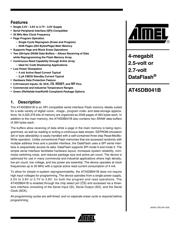
Features
• Single 2.5V - 3.6V or 2.7V - 3.6V Supply
• Serial Peripheral Interface (SPI) Compatible
• 20 MHz Max Clock Frequency
• Page Program Operation
– Single Cycle Reprogram (Erase and Program)
– 2048 Pages (264 Bytes/Page) Main Memory
• Supports Page and Block Erase Operations
• Two 264-byte SRAM Data Buffers – Allows Receiving of Data
while Reprogramming the Flash Memory Array
• Continuous Read Capability through Entire Array
– Ideal for Code Shadowing Applications
• Low Power Dissipation
– 4 mA Active Read Current Typical
– 2 µA CMOS Standby Current Typical
• Hardware Data Protection Feature
• 5.0V-tolerant Inputs: SI, SCK, CS, RESET, and WP Pins
• Commercial and Industrial Temperature Ranges
• Green (Pb/Halide-free/RoHS Compliant) Package Options
1. Description
The AT45DB041B is an SPI compatible serial interface Flash memory ideally suited
for a wide variety of digital voice-, image-, program code- and data-storage applica-
tions. Its 4,325,376 bits of memory are organized as 2048 pages of 264 bytes each. In
addition to the main memory, the AT45DB041B also contains two SRAM data buffers
of 264 bytes each.
The buffers allow receiving of data while a page in the main memory is being repro-
grammed, as well as reading or writing a continuous data stream. EEPROM emulation
(bit or byte alterability) is easily handled with a self-contained three step Read-Modify-
Write operation. Unlike conventional Flash memories that are accessed randomly with
multiple address lines and a parallel interface, the DataFlash uses a SPI serial inter-
face to sequentially access its data. DataFlash supports SPI mode 0 and mode 3. The
simple serial interface facilitates hardware layout, increases system reliability, mini-
mizes switching noise, and reduces package size and active pin count. The device is
optimized for use in many commercial and industrial applications where high density,
low pin count, low voltage, and low power are essential. The device operates at clock
frequencies up to 20 MHz with a typical active read current consumption of 4 mA.
To allow for simple in-system reprogrammability, the AT45DB041B does not require
high input voltages for programming. The device operates from a single power supply,
2.5V to 3.6V or 2.7V to 3.6V, for both the program and read operations. The
AT45DB041B is enabled through the chip select pin (CS
) and accessed via a three-
wire interface consisting of the Serial Input (SI), Serial Output (SO), and the Serial
Clock (SCK).
All programming cycles are self-timed, and no separate erase cycle is required before
programming.
4-megabit
2.5-volt or
2.7-volt
DataFlash
®
AT45DB041B
3443C–DFLSH–5/05
器件 Datasheet 文档搜索
AiEMA 数据库涵盖高达 72,405,303 个元件的数据手册,每天更新 5,000 多个 PDF 文件
