Datasheet 搜索 > Flash芯片 > Adesto Technologies > AT45DB081E-SSHN2B-T 数据手册 > AT45DB081E-SSHN2B-T 数据手册 2/70 页
 器件3D模型
¥ 9.283
AT45DB081E-SSHN2B-T 数据手册 - Adesto Technologies
制造商:
Adesto Technologies
分类:
Flash芯片
封装:
SOIC-8
描述:
闪存, DataFlash, 串行NOR, 8Mbit, 4096 Pages x 256Byte, SPI, NSOIC-8
Pictures:
3D模型
符号图
焊盘图
引脚图
产品图
页面导航:
引脚图在P2P3Hot
原理图在P4P54P55
封装尺寸在P66P67P68
型号编码规则在P35P63P64
封装信息在P63P66
技术参数、封装参数在P46
应用领域在P27
电气规格在P46
型号编号列表在P63
导航目录
AT45DB081E-SSHN2B-T数据手册
Page:
of 70 Go
若手册格式错乱,请下载阅览PDF原文件
2
AT45DB081E
DS-45DB081E-028G–DFLASH–5/2015
Description
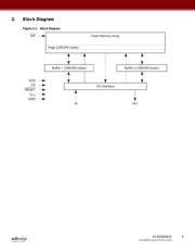
The AT45DB081E is a 1.7V minimum, serial-interface sequential access Flash memory ideally suited for a wide variety of
digital voice, image, program code, and data storage applications. The AT45DB081E also supports the RapidS serial
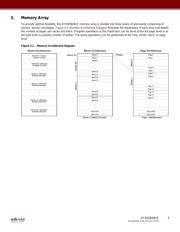
interface for applications requiring very high speed operation. Its 8,650,752 bits of memory are organized as 4,096 pages
of 256 bytes or 264 bytes each. In addition to the main memory, the AT45DB081E also contains two SRAM buffers of
256/264 bytes each. The buffers allow receiving of data while a page in the main memory is being reprogrammed.
Interleaving between both buffers can dramatically increase a system's ability to write a continuous data stream. In
addition, the SRAM buffers can be used as additional system scratch pad memory, and E
2
PROM emulation (bit or byte
alterability) can be easily handled with a self-contained three step read-modify-write operation.
Unlike conventional Flash memories that are accessed randomly with multiple address lines and a parallel interface, the
DataFlash
®
uses a serial interface to sequentially access its data. The simple sequential access dramatically reduces
active pin count, facilitates simplified hardware layout, increases system reliability, minimizes switching noise, and
reduces package size. The device is optimized for use in many commercial and industrial applications where
high-density, low-pin count, low-voltage, and low-power are essential.
To allow for simple in-system re-programmability, the AT45DB081E does not require high input voltages for
programming. The device operates from a single 1.7V to 3.6V power supply for the erase and program and read
operations. The AT45DB081E is enabled through the Chip Select pin (CS
) and accessed via a 3-wire interface consisting
of the Serial Input (SI), Serial Output (SO), and the Serial Clock (SCK).
All programming and erase cycles are self-timed.
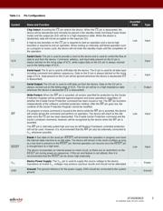
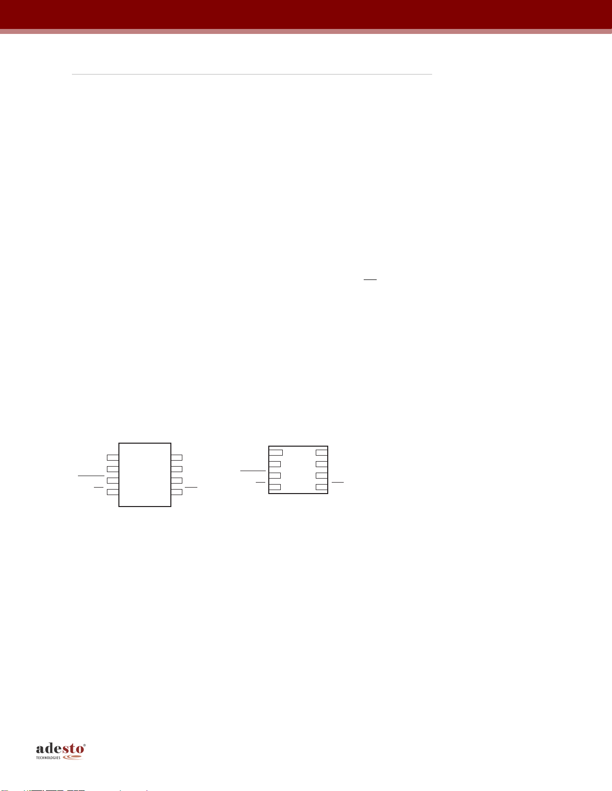
1. Pin Configurations and Pinouts
Figure 1-1. Pinouts
Note: 1. The metal pad on the bottom of the UDFN package is not internally connected to a voltage potential.
This pad can be a “no connect” or connected to GND.
1
2
3
4
8
7
6
5
SI
SCK
RESET
CS
SO
GND
V
CC
WP
8-lead SOIC
Top View
SI
SCK
RESET
CS
SO
GND
V
CC
WP
8
7
6
5
1
2
3
4
8-pad UDFN
Top View
(through package)
器件 Datasheet 文档搜索
AiEMA 数据库涵盖高达 72,405,303 个元件的数据手册,每天更新 5,000 多个 PDF 文件
