Datasheet 搜索 > Flash芯片 > Adesto Technologies > AT45DB081E-SSHN2B-T 数据手册 > AT45DB081E-SSHN2B-T 数据手册 5/70 页
 器件3D模型
¥ 9.283
AT45DB081E-SSHN2B-T 数据手册 - Adesto Technologies
制造商:
Adesto Technologies
分类:
Flash芯片
封装:
SOIC-8
描述:
闪存, DataFlash, 串行NOR, 8Mbit, 4096 Pages x 256Byte, SPI, NSOIC-8
Pictures:
3D模型
符号图
焊盘图
引脚图
产品图
页面导航:
引脚图在P2P3Hot
原理图在P4P54P55
封装尺寸在P66P67P68
型号编码规则在P35P63P64
封装信息在P63P66
技术参数、封装参数在P46
应用领域在P27
电气规格在P46
型号编号列表在P63
导航目录
AT45DB081E-SSHN2B-T数据手册
Page:
of 70 Go
若手册格式错乱,请下载阅览PDF原文件
5
AT45DB081E
DS-45DB081E-028G–DFLASH–5/2015
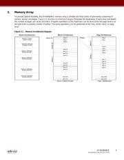
3. Memory Array
To provide optimal flexibility, the AT45DB081E memory array is divided into three levels of granularity comprising of
sectors, blocks, and pages. Figure 3-1, Memory Architecture Diagram illustrates the breakdown of each level and details
the number of pages per sector and block. Program operations to the DataFlash can be done at the full page level or at
the byte level (a variable number of bytes). The erase operations can be performed at the chip, sector, block, or page
level.
Figure 3-1. Memory Architecture Diagram
Sector 0a = 8 pages
2,048/2,112 bytes
Sector 0b = 248 pages
63,488/65,472 bytes
Block = 2,048/2,112 bytes
8 Pages
Sector 0a
Sector 0b
Page = 256/264 bytes
Page 0
Page 1
Page 6
Page 7
Page 8
Page 9
Page 4,094
Page 4,095
Block 0
Page 14
Page 15
Page 16
Page 17
Page 18
Block 1
Sector Architecture Block Architecture Page Architecture
Block 0
Block 1
Block 30
Block 31
Block 32
Block 33
Block 510
Block 511
Block 62
Block 63
Block 64
Block 65
Sector 1
Sector 15 = 256 pages
65,536/67,584 bytes
Block 2
Sector 1 = 256 pages
65,536/67,584 bytes
Sector 14 = 256 pages
65,536/67,584 bytes
Sector 2 = 256 pages
65,536/67,584 bytes
器件 Datasheet 文档搜索
AiEMA 数据库涵盖高达 72,405,303 个元件的数据手册,每天更新 5,000 多个 PDF 文件
