Datasheet 搜索 > 微控制器 > ATMEL(爱特美尔) > AT89LP52-20JU 数据手册 > AT89LP52-20JU 数据手册 5/118 页
 器件3D模型
¥ 10.569
AT89LP52-20JU 数据手册 - ATMEL(爱特美尔)
制造商:
ATMEL(爱特美尔)
分类:
微控制器
封装:
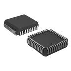
PLCC-44
Pictures:
3D模型
符号图
焊盘图
引脚图
产品图
页面导航:
导航目录
AT89LP52-20JU数据手册
Page:
of 118 Go
若手册格式错乱,请下载阅览PDF原文件
5
3709D–MICRO–12/11
AT89LP51/52
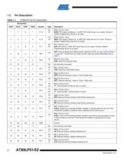
21 27 24 21 P2.3
I/O
O
P2.3: I/O Port 2 b it 3.
A11: External memory interface Address bit 11.
22 28 25 22 P2.4
I/O
O
P2.4: I/O Port 2 b it 5.
A12: External memory interface Address bit 12.
23 29 26 23 P2.5
I/O
O
P2.5: I/O Port 2 b it 5.
A13: External memory interface Address bit 13.
24 30 27 24 P2.6
I/O
O
P2.6: I/O Port 2 b it 6.
A14: External memory interface Address bit 14.
25 31 28 25 P2.7
I/O
O
P2.7: I/O Port 2 b it 7.
A15: External memory interface Address bit 15.
26 32 29 26 P4.5
I/O
O
P4.5: I/O Port 4 b it 5.
PSEN
: External memory interface Program Store Enable (active-low).
27 33 30 27 P4.4
I/O
O
P4.4: I/O Port 4 b it 4.
ALE: External memory interface Address Latch Enable.
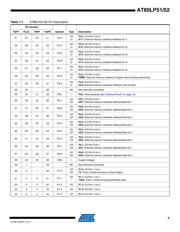
28 34 28 NC Not internally connected
29 35 31 29 POL I POL: Reset polarity (See “External Reset” on page 33.)
30 36 32 30 P0.7
I/O
I/O
P0.7: I/O Port 0 b it 7.
AD7: External memory interface Address/Data bit 7.
31 37 33 31 P0.6
I/O
I/O
P0.6: I/O Port 0 b it 6.
AD6: External memory interface Address/Data bit 6.
32 38 34 32 P0.5
I/O
I/O
P0.5: I/O Port 0 b it 5.
AD5: External memory interface Address/Data bit 5.
33 39 35 33 P0.4
I/O
I/O
P0.4: I/O Port 0 b it 4.
AD4: External memory interface Address/Data bit 4.
34 40 36 34 P0.3
I/O
I/O
P0.3: I/O Port 0 b it 3.
AD3: External memory interface Address/Data bit 3.
35 41 37 35 P0.2
I/O
I/O
P0.2: I/O Port 0 b it 2.
AD2: External memory interface Address/Data bit 2.
36 42 38 36 P0.1
I/O
I/O
P0.1: I/O Port 0 b it 1.
AD1: External memory interface Address/Dat
a bit 1.
37 43 39 37 P0.0
I/O
I/O
P0.0: I/O Port 0 b it 0.
AD0: External memory interface Address/Data bit 0.
38 44 40 38 VDD I Supply Voltage
39 1 39 NC Not internally connected
40 2 1 40 P1.0
I/O
I/O
P1.0: I/O Port 1 b it 0.
T2: Timer 2 External Input or Clock Output.
41 3 2 41 P1.1
I/O
I
P1.1: I/O Port 1 b it 1.
T2EX: Timer 2 External Capture/Reload Input.
42 4 3 42 P1.2 I/O P1.2: I/O Port 1 b it 2.
43 5 4 43 P1.3 I/O P1.3: I/O Port 1 b it 3.
44 6 5 44 P1.4 I/O P1.4: I/O Port 1 b it 4.
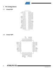
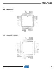
Table 1-1. AT89LP51/52 Pin Description
Pin Number
Symbol Type DescriptionTQFP PLCC PDIP VQFN
器件 Datasheet 文档搜索
AiEMA 数据库涵盖高达 72,405,303 个元件的数据手册,每天更新 5,000 多个 PDF 文件
