Datasheet 搜索 > 8位微控制器 > ATMEL(爱特美尔) > ATMEGA128A-AU 数据手册 > ATMEGA128A-AU 数据手册 124/386 页
 器件3D模型
¥ 15.026
ATMEGA128A-AU 数据手册 - ATMEL(爱特美尔)
制造商:
ATMEL(爱特美尔)
分类:
8位微控制器
封装:
TQFP-64
描述:
ATMEL ATMEGA128A-AU 微控制器, 8位, 低功率高性能, ATmega, 16 MHz, 128 KB, 4 KB, 64 引脚, TQFP
Pictures:
3D模型
符号图
焊盘图
引脚图
产品图
页面导航:
引脚图在P2P5P67P93P112P148Hot
原理图在P3P9P65P93P95P96P97P113P119P120P122P124
封装尺寸在P373P374
型号编码规则在P372P378
封装信息在P373
应用领域在P27P51P60P63P277P281P288P291P292
电气规格在P90P378
导航目录
ATMEGA128A-AU数据手册
Page:
of 386 Go
若手册格式错乱,请下载阅览PDF原文件
124
8151H–AVR–02/11
ATmega128A
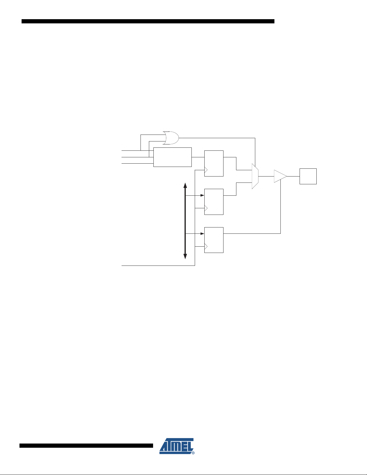
15.8 Compare Match Output Unit
The Compare Output mode (COMnx1:0) bits have two functions. The waveform generator uses
the COMnx1:0 bits for defining the output compare (OCnx) state at the next compare match.
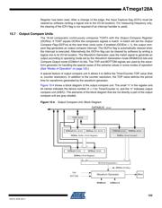
Secondly the COMnx1:0 bits control the OCnx pin output source. Figure 15-5 shows a simplified
schematic of the logic affected by the COMnx1:0 bit setting. The I/O registers, I/O bits, and I/O
pins in the figure are shown in bold. Only the parts of the general I/O port control registers (DDR
and PORT) that are affected by the COMnx1:0 bits are shown. When referring to the OCnx
state, the reference is for the internal OCnx Register, not the OCnx pin. If a system Reset occur,
the OCnx Register is reset to “0”.
Figure 15-5. Compare Match Output Unit, Schematic
The general I/O port function is overridden by the output compare (OCnx) from the Waveform
Generator if either of the COMnx1:0 bits are set. However, the OCnx pin direction (input or out-
put) is still controlled by the Data Direction Register (DDR) for the port pin. The data direction
register bit for the OCnx pin (DDR_OCnx) must be set as output before the OCnx value is visible
on the pin. The port override function is generally independent of the waveform generation
mode, but there are some exceptions. Refer to Table 15-2, Table 15-3 and Table 15-4 for
details.
The design of the output compare pin logic allows initialization of the OCnx state before the out-
put is enabled. Note that some COMnx1:0 bit settings are reserved for certain modes of
operation. See “Register Description” on page 134.
The COMnx1:0 bits have no effect on the Input Capture unit.
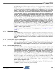
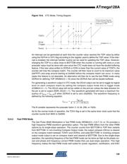
15.8.1 Compare Output Mode and Waveform Generation
The waveform generator uses the COMnx1:0 bits differently in normal, CTC, and PWM modes.
For all modes, setting the COMnx1:0 = 0 tells the waveform generator that no action on the
OCnx Register is to be performed on the next compare match. For compare output actions in the
non-PWM modes refer to Table 15-2 on page 135. For fast PWM mode refer to Table 15-3 on
page 135, and for phase correct and phase and frequency correct PWM refer to Table 15-4 on
page 136.
PORT
DDR
DQ
DQ
OCnx
Pin
OCnx
DQ
Waveform
Generator
COMnx1
COMnx0
0
1
DATA BU S
FOCnx
clk
I/O
器件 Datasheet 文档搜索
AiEMA 数据库涵盖高达 72,405,303 个元件的数据手册,每天更新 5,000 多个 PDF 文件
