Datasheet 搜索 > 微控制器 > Microchip(微芯) > ATMEGA8515L-8AU 数据手册 > ATMEGA8515L-8AU 数据手册 59/257 页
 器件3D模型
¥ 24.835
ATMEGA8515L-8AU 数据手册 - Microchip(微芯)
制造商:
Microchip(微芯)
分类:
微控制器
封装:
TQFP-44
描述:
8 位 megaAVR 微控制器,4KB 到 16KB 闪存我们在 RS Components 提供 Atmel 的各种 megaAVR 8 位微控制器。每个微控制器均基于增强型 RISC 体系结构,并具有 QTouch 库支持。 所有 megaAVR 微控制器具有不同 Kb 的系统内可编程内存、EEPROM 和 SRAM 以及不同引脚和封装类型。 **megaAVR 8 位微控制器类型 ** ATmega8 ATmega16 ATmega48 ATmega88 ATmega162 ATmega164 ATmega165 ATmega168 ATmega8515 ATmega8535
Pictures:
3D模型
符号图
焊盘图
引脚图
产品图
页面导航:
引脚图在P2P5P61P97Hot
原理图在P3P8P59P80P81P82P84P98P103P104P106P108
封装尺寸在P245P246P247P248
型号编码规则在P244
封装信息在P245P251
应用领域在P31P45P54P57P166P169P179P180
电气规格在P59P251
导航目录
ATMEGA8515L-8AU数据手册
Page:
of 257 Go
若手册格式错乱,请下载阅览PDF原文件
59
ATmega8515(L)
2512J–AVR–10/06
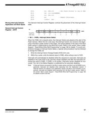
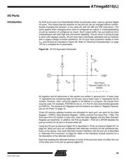
I/O Ports
Introduction All AVR ports have true Read-Modify-Write functionality when used as general digital
I/O ports. This means that the direction of one port pin can be changed without uninten-
tionally changing the direction of any other pin with the SBI and CBI instructions. The
same applies when changing drive value (if configured as output) or enabling/disabling
of pull-up resistors (if configured as input). Each output buffer has symmetrical drive
characteristics with both high sink and source capability. The pin driver is strong enough
to drive LED displays directly. All port pins have individually selectable pull-up resistors
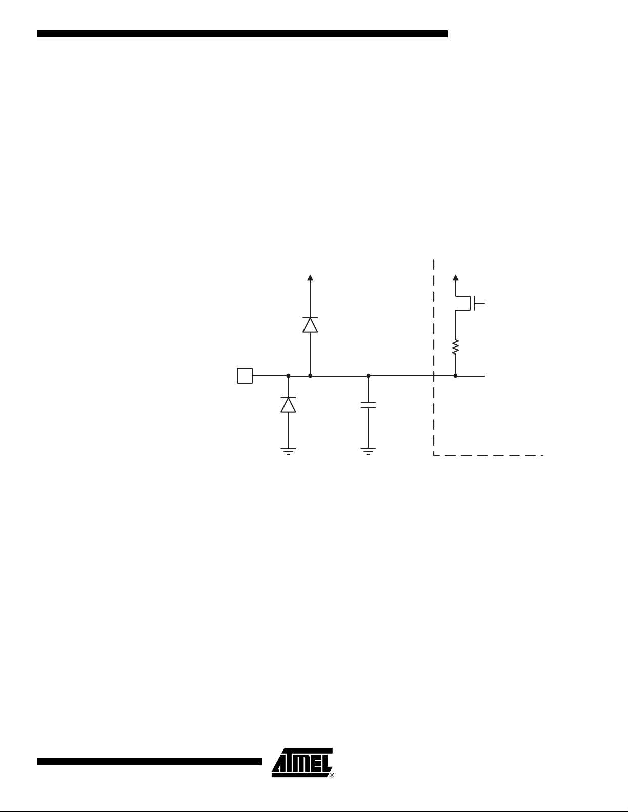
with a supply-voltage invariant resistance. All I/O pins have protection diodes to both
V
CC
and Ground as indicated in Figure 29. Refer to “Electrical Characteristics” on page
197 for a complete list of parameters.
Figure 29. I/O Pin Equivalent Schematic
All registers and bit references in this section are written in general form. A lower case
“x” represents the numbering letter for the port, and a lower case “n” represents the bit
number. However, when using the register or bit defines in a program, the precise form
must be used. For example, PORTB3 for bit no. 3 in Port B, here documented generally
as PORTxn. The physical I/O Registers and bit locations are listed in “Register Descrip-
tion for I/O Ports” on page 75.
Three I/O memory address locations are allocated for each port, one each for the Data
Register – PORTx, Data Direction Register – DDRx, and the Port Input Pins – PINx. The
Port Input Pins I/O location is read only, while the Data Register and the Data Direction
Register are read/write. In addition, the Pull-up Disable – PUD bit in SFIOR disables the
pull-up function for all pins in all ports when set.
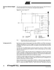
Using the I/O port as General Digital I/O is described in “Ports as General Digital I/O” on
page 60. Most port pins are multiplexed with alternate functions for the peripheral fea-
tures on the device. How each alternate function interferes with the port pin is described
in “Alternate Port Functions” on page 64. Refer to the individual module sections for a
full description of the alternate functions.
Note that enabling the alternate function of some of the port pins does not affect the use
of the other pins in the port as general digital I/O.
C
pin
Logic
R
pu
See Figure
"General Digital I/O" fo
r
Details
Pxn
器件 Datasheet 文档搜索
AiEMA 数据库涵盖高达 72,405,303 个元件的数据手册,每天更新 5,000 多个 PDF 文件
