Datasheet 搜索 > 微控制器 > Microchip(微芯) > ATMEGA8515L-8AU 数据手册 > ATMEGA8515L-8AU 数据手册 60/257 页
 器件3D模型
¥ 24.857
ATMEGA8515L-8AU 数据手册 - Microchip(微芯)
制造商:
Microchip(微芯)
分类:
微控制器
封装:
TQFP-44
描述:
8 位 megaAVR 微控制器,4KB 到 16KB 闪存我们在 RS Components 提供 Atmel 的各种 megaAVR 8 位微控制器。每个微控制器均基于增强型 RISC 体系结构,并具有 QTouch 库支持。 所有 megaAVR 微控制器具有不同 Kb 的系统内可编程内存、EEPROM 和 SRAM 以及不同引脚和封装类型。 **megaAVR 8 位微控制器类型 ** ATmega8 ATmega16 ATmega48 ATmega88 ATmega162 ATmega164 ATmega165 ATmega168 ATmega8515 ATmega8535
Pictures:
3D模型
符号图
焊盘图
引脚图
产品图
页面导航:
引脚图在P2P5P61P97Hot
原理图在P3P8P59P80P81P82P84P98P103P104P106P108
封装尺寸在P245P246P247P248
型号编码规则在P244
封装信息在P245P251
应用领域在P31P45P54P57P166P169P179P180
电气规格在P59P251
导航目录
ATMEGA8515L-8AU数据手册
Page:
of 257 Go
若手册格式错乱,请下载阅览PDF原文件
60
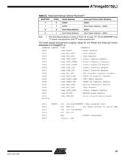
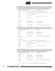
ATmega8515(L)
2512J–AVR–10/06
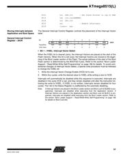
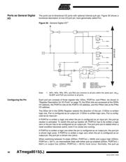
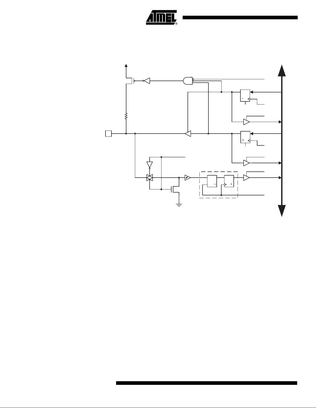
Ports as General Digital
I/O
The ports are bi-directional I/O ports with optional internal pull-ups. Figure 30 shows a
functional description of one I/O-port pin, here generically called Pxn.
Figure 30. General Digital I/O
(1)
Note: 1. WPx, WDx, RRx, RPx, and RDx are common to all pins within the same port. clk
I/O
,
SLEEP, and PUD are common to all ports.
Configuring the Pin Each port pin consists of three register bits: DDxn, PORTxn, and PINxn. As shown in
“Register Description for I/O Ports” on page 75, the DDxn bits are accessed at the DDRx
I/O address, the PORTxn bits at the PORTx I/O address, and the PINxn bits at the PINx
I/O address.
The DDxn bit in the DDRx Register selects the direction of this pin. If DDxn is written
logic one, Pxn is configured as an output pin. If DDxn is written logic zero, Pxn is config-
ured as an input pin.
If PORTxn is written a logic one when the pin is configured as an input pin, the pull-up
resistor is activated. To switch the pull-up resistor off, PORTxn has to be written a logic
zero or the pin has to be configured as an output pin. The port pins are tri-stated when a
reset condition becomes active, even if no clocks are running.
If PORTxn is written a logic one when the pin is configured as an output pin, the port pin
is driven high (one). If PORTxn is written a logic zero when the pin is configured as an
output pin, the port pin is driven low (zero).
When switching between tri-state ({DDxn, PORTxn} = 0b00) and output high ({DDxn,
PORTxn} = 0b11), an intermediate state with either pull-up enabled ({DDxn, PORTxn} =
0b01) or output low ({DDxn, PORTxn} = 0b10) must occur. Normally, the pull-up
clk
RPx
RRx
WPx
RDx
WDx
PUD
SYNCHRONIZER
WDx: WRITE DDRx
WPx: WRITE PORTx
RRx: READ PORTx REGISTER
RPx: READ PORTx PIN
PUD: PULLUP DISABLE
clk
I/O
: I/O CLOCK
RDx: READ DDRx
D
L
Q
Q
RESET
RESET
Q
Q
D
Q
Q
D
CLR
PORTxn
Q
Q
D
CLR
DDxn
PINxn
DATA B U S
SLEEP
SLEEP: SLEEP CONTROL
Pxn
I/O
器件 Datasheet 文档搜索
AiEMA 数据库涵盖高达 72,405,303 个元件的数据手册,每天更新 5,000 多个 PDF 文件
