Datasheet 搜索 > ATMEL(爱特美尔) > ATSENSE301HA-AUR 数据手册 > ATSENSE301HA-AUR 数据手册 12/59 页
 器件3D模型
¥ 25.168
ATSENSE301HA-AUR 数据手册 - ATMEL(爱特美尔)
制造商:
ATMEL(爱特美尔)
封装:
TQFP-32
Pictures:
3D模型
符号图
焊盘图
引脚图
产品图
页面导航:
导航目录
ATSENSE301HA-AUR数据手册
Page:
of 59 Go
若手册格式错乱,请下载阅览PDF原文件
12
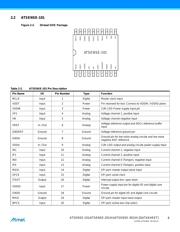
ATSENSE-101/ATSENSE-201(H)/ATSENSE-301(H) [DATASHEET]
11219B–ATSENSE–20-Feb-14
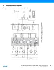
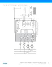
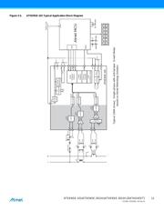
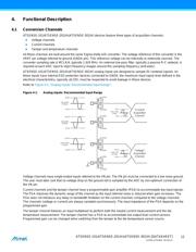
4. Functional Description
4.1 Conversion Channels
ATSENSE-101/ATSENSE-201(H)/ATSENSE-301(H) devices feature three types of acquisition channels:
Voltage channels
Current channels
Tamper and temperature channels
All these channels are built around the same Sigma-Delta A/D converter. The voltage reference of this converter is the
VREF pin voltage referred to ground (GNDA pin). This reference voltage can be internally or externally sourced. The
converter sampling rate is MCLK/4, typically 1.024 MHz. An external low-pass filter, typically a passive R-C network, is
required at each ADC input to reject frequency images around this sampling frequency (anti-alias).
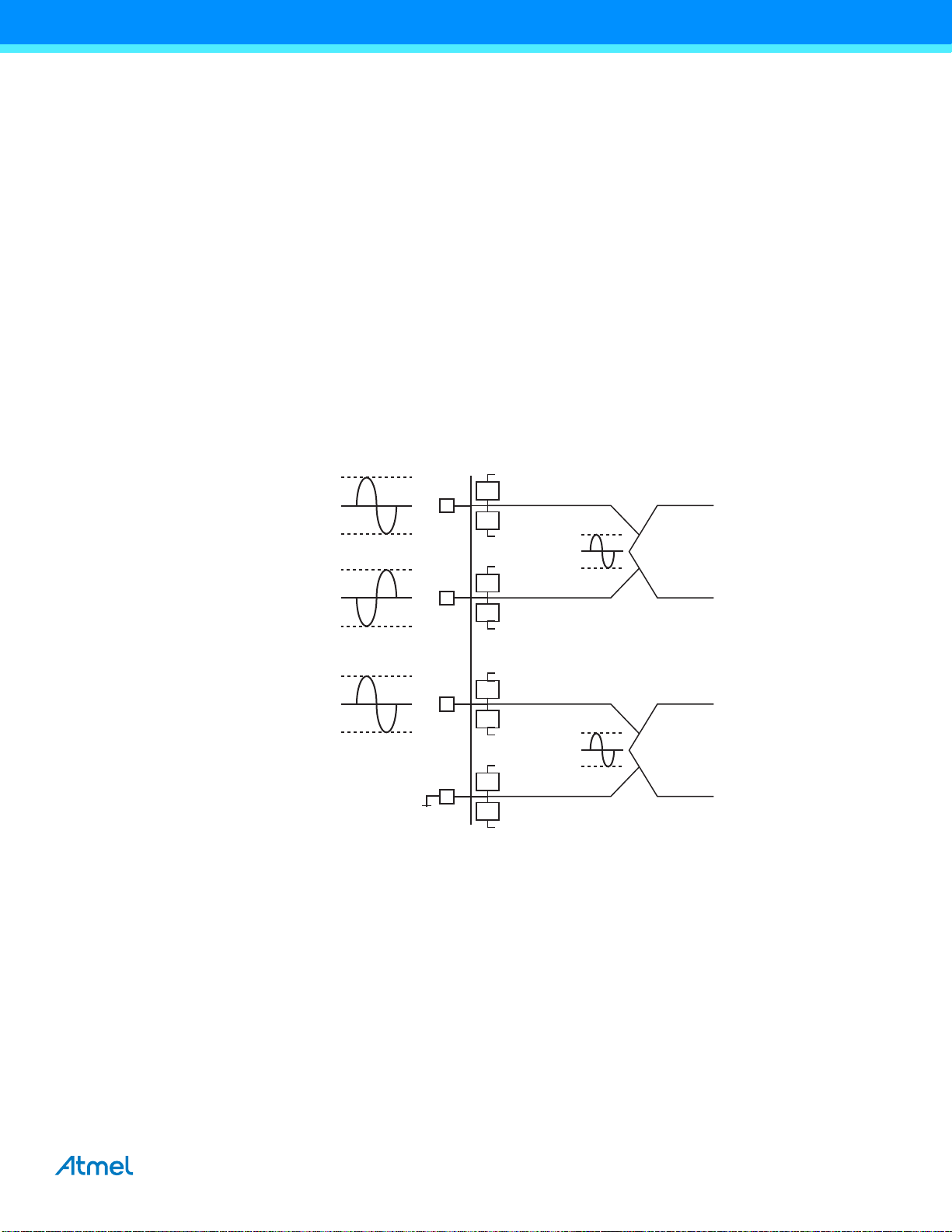
ATSENSE-101/ATSENSE-201(H)/ATSENSE-301(H) analog inputs are designed to sample 0V centered signals. As
these inputs have internal ESD protection devices connected to GNDA, the maximum input signal level defined in the
electrical characteristics, typically ±0.25V, must be respected to avoid leakage in these devices.
Refer to Figure 4-1, "Analog Inputs: Recommended Input Range".
Figure 4-1. Analog Inputs: Recommended Input Range
Voltage channels have single-ended inputs referred to the VN pin. The VN pin must be connected to a low noise ground.
The user must take care that no voltage drop on the ground net is sampled by the ADC by non-optimum connection of
the VN pin.
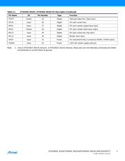
Current channels and the tamper channel have a programmable gain amplifier (PGA) to accommodate low input signals.
The PGA improves the dynamic range of the channel as the input referred noise is reduced when gain increases. The
PGA does not introduce any delay or bandwidth limitation on the current channels compared to the voltage channels.
The channels (voltage or current) are always sampled synchronously. The input impedance of the PGA depends on the
programmed gain.
The tamper channel features an input multiplexer to perform both the neutral current measurement and the die
temperature measurement. The tamper channel has a PGA to accommodate low output level current sensors.
Programmed gain can be changed when switching from the tamper to the die temperature sensor source.
+0.25V
-0.25V
+0.25V
-0.25V
IPx
INx
E.S.D
E.S.D
VDDA
GNDA
E.S.D
E.S.D
VDDA
GNDA
“Current”
Acquisition
Channel
+0.5V
-0.5V
V(IPx,GND)
(0.5Vpp)
V(INx,GND)
(0.5Vpp)
V(IPx,VINx)
(1Vpp)
+0.25V
-0.25V
VPx
VN
E.S.D
E.S.D
VDDA
GNDA
E.S.D
E.S.D
VDDA
GNDA
“Voltage”
Acquisition
Channel
+0.25V
-0.25V
V(VPx,GND)
(0.5Vpp)
V(VPx,VN)
(0.5Vpp)
GND
器件 Datasheet 文档搜索
AiEMA 数据库涵盖高达 72,405,303 个元件的数据手册,每天更新 5,000 多个 PDF 文件
