Datasheet 搜索 > 电池管理芯片 > TI(德州仪器) > BQ29209DRBR 数据手册 > BQ29209DRBR 数据手册 2/17 页
 器件3D模型
¥ 2.428
BQ29209DRBR 数据手册 - TI(德州仪器)
制造商:
TI(德州仪器)
分类:
电池管理芯片
封装:
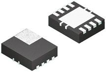
VSON EP-8
描述:
Texas Instruments锂离子电池保护 IC 可检测各种故障条件,如过压、欠压、放电过电流和短路。 需要在没有监控器时提供独立保护或补充安全。### 电池管理,Texas Instruments
Pictures:
3D模型
符号图
焊盘图
引脚图
产品图
页面导航:
导航目录
BQ29209DRBR数据手册
Page:
of 17 Go
若手册格式错乱,请下载阅览PDF原文件
bq29200
bq29209
SLUSA52A –SEPTEMBER 2010–REVISED NOVEMBER 2010
www.ti.com
These devices have limited built-in ESD protection. The leads should be shorted together or the device placed in conductive foam
during storage or handling to prevent electrostatic damage to the MOS gates.
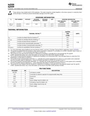
ORDERING INFORMATION
T
A
PART NUMBER PACKAGE PACKAGE PACKAGE OVP ORDERING INFORMATION
DESIGNATOR MARKING
TAPE AND REEL TAPE AND REEL
(LARGE) (SMALL)
–40°C to BQ29200 QFN-8 DRB 200 4.35 V BQ29200DRBR BQ29209DRBT
+110°C
BQ29209 209 4.30 V BQ29209DRBR BQ29209DRBT
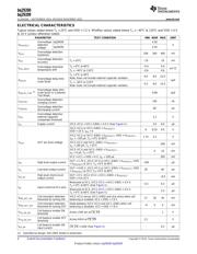
THERMAL INFORMATION
bq2920x
THERMAL METRIC
(1)
DRB UNITS
8 PINS
q
JA
Junction-to-ambient thermal resistance
(2)
50.5
q
JC(top)
Junction-to-case(top) thermal resistance
(3)
25.1
q
JB
Junction-to-board thermal resistance
(4)
19.3
°C/W
y
JT
Junction-to-top characterization parameter
(5)
0.7
y
JB
Junction-to-board characterization parameter
(6)
18.9
q
JC(bottom)
Junction-to-case(bottom) thermal resistance
(7)
5.2
(1) For more information about traditional and new thermal metrics, see the IC Package Thermal Metrics application report, SPRA953.
(2) The junction-to-ambient thermal resistance under natural convection is obtained in a simulation on a JEDEC-standard, high-K board, as
specified in JESD51-7, in an environment described in JESD51-2a.
(3) The junction-to-case (top) thermal resistance is obtained by simulating a cold plate test on the package top. No specific
JEDEC-standard test exists, but a close description can be found in the ANSI SEMI standard G30-88.
(4) The junction-to-board thermal resistance is obtained by simulating in an environment with a ring cold plate fixture to control the PCB
temperature, as described in JESD51-8.
(5) The junction-to-top characterization parameter, y
JT
, estimates the junction temperature of a device in a real system and is extracted
from the simulation data for obtaining q
JA
, using a procedure described in JESD51-2a (sections 6 and 7).
(6) The junction-to-board characterization parameter, y
JB
, estimates the junction temperature of a device in a real system and is extracted
from the simulation data for obtaining q
JA
, using a procedure described in JESD51-2a (sections 6 and 7).
(7) The junction-to-case (bottom) thermal resistance is obtained by simulating a cold plate test on the exposed (power) pad. No specific
JEDEC standard test exists, but a close description can be found in the ANSI SEMI standard G30-88.
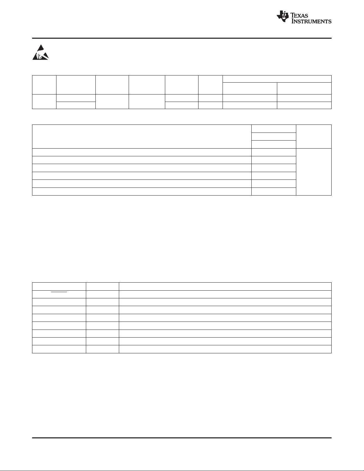
PIN FUNCTIONS
PIN NAME NO. DESCRIPTION
CB_EN 6 Cell balance enable
CD 4 Connection to external capacitor for programmable delay time
GND 5 Ground pin
OUT 8 Output
VC1 2 Sense voltage input for bottom cell
VC1_CB 3 Cell balance input for bottom cell
VC2 1 Sense voltage input for top cell
VDD 7 Power supply
2 Submit Documentation Feedback Copyright © 2010, Texas Instruments Incorporated
Product Folder Link(s): bq29200 bq29209
器件 Datasheet 文档搜索
AiEMA 数据库涵盖高达 72,405,303 个元件的数据手册,每天更新 5,000 多个 PDF 文件
