Datasheet 搜索 > EEPROM芯片 > ON Semiconductor(安森美) > CAT24C02WI-GT3A 数据手册 > CAT24C02WI-GT3A 数据手册 4/21 页
 器件3D模型
¥ 0.29
CAT24C02WI-GT3A 数据手册 - ON Semiconductor(安森美)
制造商:
ON Semiconductor(安森美)
分类:
EEPROM芯片
封装:
SOIC-8
描述:
ON SEMICONDUCTOR CAT24C02WI-GT3A EEPROM, 2 Kbit, 256 x 8位, 400 kHz, I2C, SOIC, 8 引脚
Pictures:
3D模型
符号图
焊盘图
引脚图
产品图
页面导航:
引脚图在P1P4Hot
封装尺寸在P9P10P11P12P13P14P15P16P17P18
焊盘布局在P16P17P18
型号编码规则在P1P19P20P21
标记信息在P1P19P20P21
封装信息在P21
功能描述在P4
技术参数、封装参数在P2P21
电气规格在P2
型号编号列表在P2P19

导航目录
CAT24C02WI-GT3A数据手册
Page:
of 21 Go
若手册格式错乱,请下载阅览PDF原文件

CAT24C01, CAT24C02, CAT24C04, CAT24C08, CAT24C16
http://onsemi.com
4
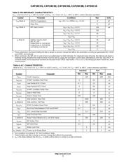
Table 7. A.C. TEST CONDITIONS
Input Drive Levels 0.2 x V
CC
to 0.8 x V
CC
Input Rise and Fall Time v 50 ns
Input Reference Levels 0.3 x V
CC
, 0.7 x V
CC
Output Reference Level 0.5 x V
CC
Output Test Load Current Source I
OL
= 3 mA (V
CC
w 2.5 V); I
OL
= 1 mA (V
CC
< 2.5 V); C
L
= 100 pF
Power−On Reset (POR)
Each CAT24Cxx* incorporates Power−On Reset (POR)
circuitry which protects the internal logic against powering
up in the wrong state.
A CAT24Cxx device will power up into Standby mode
after V
CC
exceeds the POR trigger level and will power
down into Reset mode when V
CC
drops below the POR
trigger level. This bi−directional POR feature protects the
device against ‘brown−out’ failure following a temporary
loss of power.
*For common features, the CAT24C01/02/04/08/16 will be
referred to as CAT24Cxx.
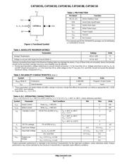
Pin Description
SCL: The Serial Clock input pin accepts the Serial Clock
generated by the Master.
SDA: The Serial Data I/O pin receives input data and
transmits data stored in EEPROM. In transmit mode, this pin
is open drain. Data is acquired on the positive edge, and is
delivered on the negative edge of SCL.
A0, A1 and A2: The Address inputs set the device address
when cascading multiple devices. When not driven, these
pins are pulled LOW internally.
WP: The Write Protect input pin inhibits all write
operations, when pulled HIGH. When not driven, this pin is
pulled LOW internally.
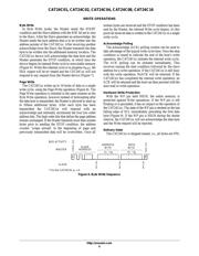
Functional Description
The CAT24Cxx supports the Inter−Integrated Circuit
(I
2
C) Bus data transmission protocol, which defines a device
that sends data to the bus as a transmitter and a device
receiving data as a receiver. Data flow is controlled by a
Master device, which generates the serial clock and all
START and STOP conditions. The CAT24Cxx acts as a
Slave device. Master and Slave alternate as either
transmitter or receiver.
I
2
C Bus Protocol
The I
2
C bus consists of two ‘wires’, SCL and SDA. The
two wires are connected to the V
CC
supply via pull−up
resistors. Master and Slave devices connect to the 2−wire
bus via their respective SCL and SDA pins. The transmitting
device pulls down the SDA line to ‘transmit’ a ‘0’ and
releases it to ‘transmit’ a ‘1’.
Data transfer may be initiated only when the bus is not
busy (see AC Characteristics).
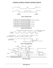
During data transfer, the SDA line must remain stable
while the SCL line is high. An SDA transition while SCL is
high will be interpreted as a START or STOP condition
(Figure 2). The START condition precedes all commands. It
consists of a HIGH to LOW transition on SDA while SCL
is HIGH. The START acts as a ‘wake−up’ call to all
receivers. Absent a START, a Slave will not respond to
commands. The STOP condition completes all commands.
It consists of a LOW to HIGH transition on SDA while SCL
is HIGH.
NOTE: The I/O pins of CAT24Cxx do not obstruct the SCL
and SDA lines if the VCC supply is switched off. During
power−up, the SCL and SDA pins (connected with pull−up
resistors to VCC) will follow the VCC monotonically from
VSS (0 V) to nominal VCC value, regardless of pull−up
resistor value. The delta between the VCC and the
instantaneous voltage levels during power ramping will be
determined by the relation between bus time constant
(determined by pull−up resistance and bus capacitance) and
actual VCC ramp rate.
Device Addressing
The Master initiates data transfer by creating a START
condition on the bus. The Master then broadcasts an 8−bit
serial Slave address. For normal Read/Write operations, the
first 4 bits of the Slave address are fixed at 1010 (Ah). The
next 3 bits are used as programmable address bits when
cascading multiple devices and/or as internal address bits.
The last bit of the slave address, R/W, specifies whether a
Read (1) or Write (0) operation is to be performed. The 3
address space extension bits are assigned as illustrated in
Figure 3. A
2
, A
1
and A
0
must match the state of the external
address pins, and a
10
, a
9
and a
8
are internal address bits.
Acknowledge
After processing the Slave address, the Slave responds
with an acknowledge (ACK) by pulling down the SDA line
during the 9th clock cycle (Figure 4). The Slave will also
acknowledge the address byte and every data byte presented
in Write mode. In Read mode the Slave shifts out a data byte,
and then releases the SDA line during the 9
th
clock cycle. As
long as the Master acknowledges the data, the Slave will
continue transmitting. The Master terminates the session by
not acknowledging the last data byte (NoACK) and by
issuing a STOP condition. Bus timing is illustrated in
Figure 5.
器件 Datasheet 文档搜索
AiEMA 数据库涵盖高达 72,405,303 个元件的数据手册,每天更新 5,000 多个 PDF 文件
