Datasheet 搜索 > RF射频器件 > TI(德州仪器) > CC1101RGPR 数据手册 > CC1101RGPR 数据手册 20/105 页
 器件3D模型
¥ 3.93
CC1101RGPR 数据手册 - TI(德州仪器)
制造商:
TI(德州仪器)
分类:
RF射频器件
封装:
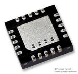
QFN-20
描述:
TEXAS INSTRUMENTS CC1101RGPR 芯片, 射频收发器, QFN-20
Pictures:
3D模型
符号图
焊盘图
引脚图
产品图
页面导航:
引脚图在P20P34P71Hot
典型应用电路图在P25
原理图在P22
封装尺寸在P99
焊盘布局在P26
型号编码规则在P95
标记信息在P99
封装信息在P99P100
焊接温度在P8
功能描述在P2
技术参数、封装参数在P8P9P34
应用领域在P1P105
电气规格在P9
导航目录
CC1101RGPR数据手册
Page:
of 105 Go
若手册格式错乱,请下载阅览PDF原文件
CC1101
SWRS061I Page 20 of 98
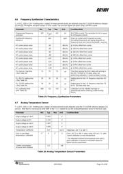
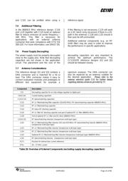
4.8 DC Characteristics
T
A
= 25C if nothing else stated.
Table 17: DC Characteristics
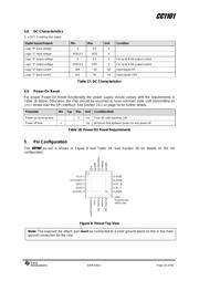
4.9 Power-On Reset
For proper Power-On-Reset functionality the power supply should comply with the requirements in
Table 18 below. Otherwise, the chip should be assumed to have unknown state until transmitting an
SRES strobe over the SPI interface. See Section 19.1 on page 50 for further details.
Table 18: Power-On Reset Requirements
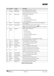
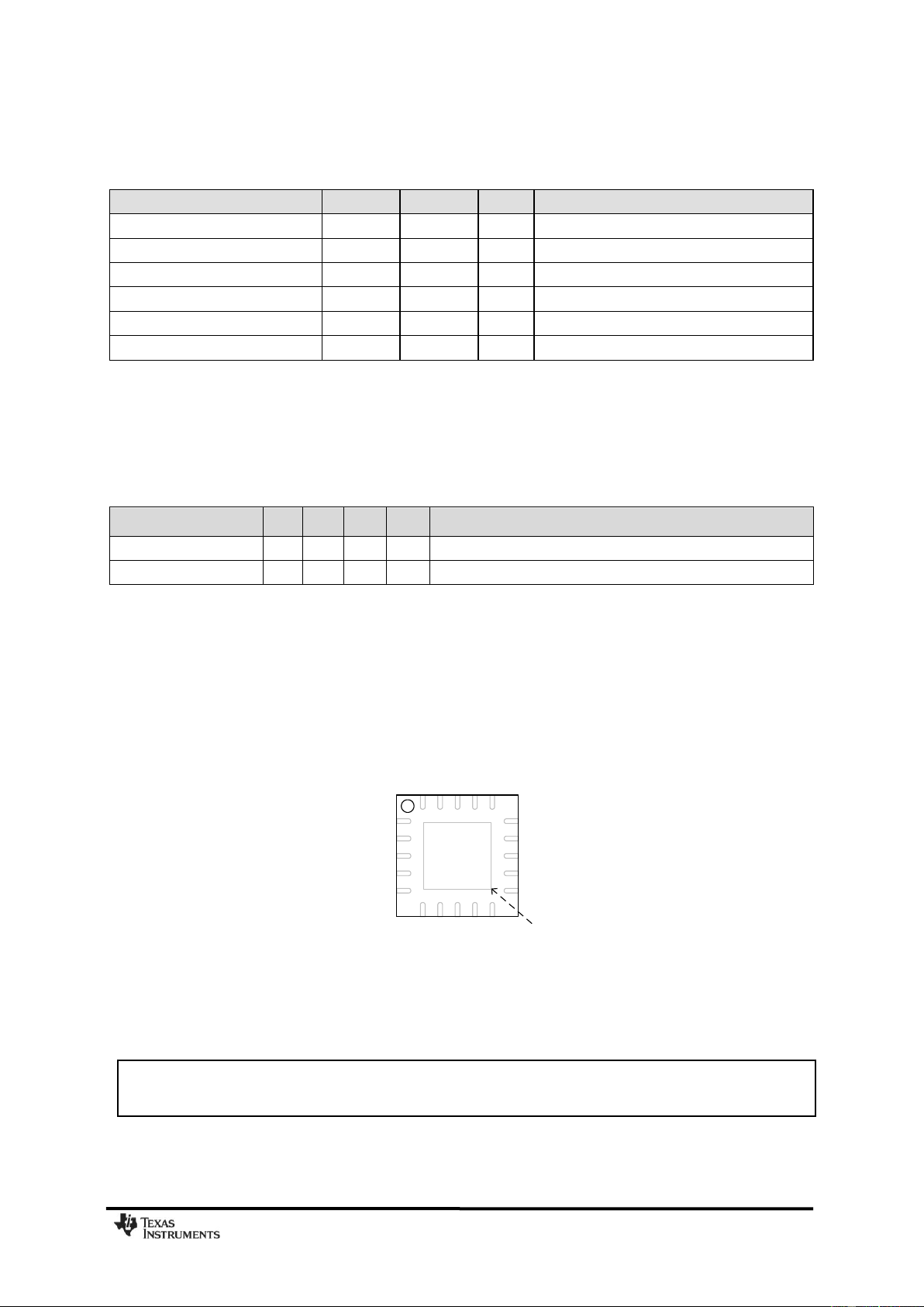
5 Pin Configuration
The
CC1101
pin-out is shown in Figure 8 and Table 19. See Section 26 for details on the I/O
configuration.
1
20 19 18 17 16
15
14
13
12
11
109876
5
4
3
2
GND
Exposed die
attach pad
SCLK
SO (GDO1)
GDO2
DVDD
DCOUPL
GDO0 (ATEST)
XOSC_Q1
AVDD
XOSC_Q2
AVDD
RF_P
RF_N
GND
AVDD
RBIAS
DGUARD
GND
SI
CSn
AVDD
Figure 8: Pinout Top View
.
Digital Inputs/Outputs
Min
Max
Unit
Condition
Logic "0" input voltage
0
0.7
V
Logic "1" input voltage
VDD-0.7
VDD
V
Logic "0" output voltage
0
0.5
V
For up to 4 mA output current
Logic "1" output voltage
VDD-0.3
VDD
V
For up to 4 mA output current
Logic "0" input current
N/A
–50
nA
Input equals 0V
Logic "1" input current
N/A
50
nA
Input equals VDD
Parameter
Min
Typ
Max
Unit
Condition/Note
Power-up ramp-up time
5
ms
From 0V until reaching 1.8V
Power off time
1
ms
Minimum time between power-on and power-off
Note: The exposed die attach pad must be connected to a solid ground plane as this is the main
ground connection for the chip
器件 Datasheet 文档搜索
AiEMA 数据库涵盖高达 72,405,303 个元件的数据手册,每天更新 5,000 多个 PDF 文件
