Datasheet 搜索 > 逻辑控制器 > TI(德州仪器) > CD4066BNSR 数据手册 > CD4066BNSR 数据手册 1/33 页
 器件3D模型
¥ 5.239
CD4066BNSR 数据手册 - TI(德州仪器)
制造商:
TI(德州仪器)
分类:
逻辑控制器
封装:
SOP-14
描述:
CMOS四路双向开关 CMOS QUAD BILATERAL SWITCH
Pictures:
3D模型
符号图
焊盘图
引脚图
产品图
页面导航:
引脚图在P3Hot
典型应用电路图在P15P16
原理图在P14
封装尺寸在P19P20P22P23P26
焊盘布局在P27
标记信息在P19P20
封装信息在P18P19P20P21P22P23
技术参数、封装参数在P4
应用领域在P1P21
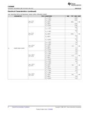
电气规格在P5P6P7P8


导航目录
CD4066BNSR数据手册
Page:
of 33 Go
若手册格式错乱,请下载阅览PDF原文件
Control
V
C
(1)
V
DD
V
SS
V
SS
n
n
p
Out
V
os
Control
Switch
In
n
p
V
is
CMOS Protection Network
Copyright © 2016, Texas Instruments Incorporated
Product
Folder
Order
Now
Technical
Documents
Tools &
Software
Support &
Community
An IMPORTANT NOTICE at the end of this data sheet addresses availability, warranty, changes, use in safety-critical applications,
intellectual property matters and other important disclaimers. PRODUCTION DATA.
CD4066B
SCHS051G –NOVEMBER 1998–REVISED JUNE 2017
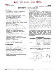
CD4066B CMOS Quad Bilateral Switch
1
1 Features
1
• 15-V Digital or ±7.5-V Peak-to-Peak Switching
• 125-Ω Typical On-State Resistance for
15-V Operation
• Switch On-State Resistance Matched to Within
5 Ω Over 15-V Signal-Input Range
• On-State Resistance Flat Over Full
Peak-to-Peak Signal Range
• High ON/OFF Output-Voltage Ratio:
80 dB Typical at f
is
= 10 kHz, R
L
= 1 kΩ
• High Degree of Linearity: <0.5% Distortion Typical
at f
is
= 1 kHz, V
is
= 5 V
p-p
V
DD
– V
SS
≥ 10 V, R
L
= 10 kΩ
• Extremely Low Off-State Switch Leakage,
Resulting in Very Low Offset Current and High
Effective Off-State Resistance: 10 pA Typical at
V
DD
– V
SS
= 10 V, T
A
= 25 ° C
• Extremely High Control Input Impedance
(Control Circuit Isolated From Signal Circuit):
10
12
Ω Typical
• Low Crosstalk Between Switches: –50 dB Typical
at f
is
= 8 MHz, R
L
= 1 kΩ
• Matched Control-Input to Signal-Output
Capacitance: Reduces Output Signal Transients
• Frequency Response,
Switch On = 40 MHz Typical
• 100% Tested for Quiescent Current at 20 V
• 5-V, 10-V, and 15-V Parametric Ratings
2 Applications
• Analog Signal Switching/Multiplexing: Signal
Gating, Modulators, Squelch Controls,
Demodulators, Choppers, Commutating Switches
• Digital Signal Switching/Multiplexing
• Transmission-Gate Logic Implementation
• Analog-to-Digital and Digital-to-Analog
Conversions
• Digital Control of Frequency, Impedance, Phase,
and Analog-Signal Gain
3 Description
The CD4066B device is a quad bilateral switch
intended for the transmission or multiplexing of
analog or digital signals. It is pin-for-pin compatible
with the CD4016B device, but exhibits a much lower
on-state resistance. In addition, the on-state
resistance is relatively constant over the full signal-
input range.
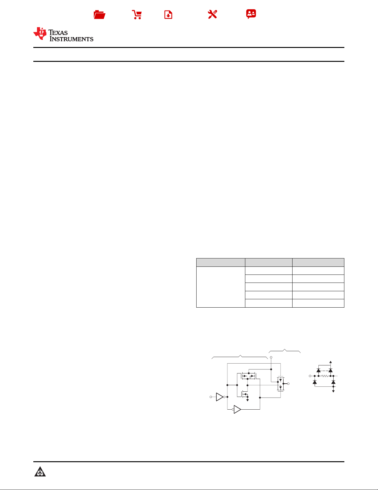
The CD4066B device consists of four bilateral
switches, each with independent controls. Both the p
and the n devices in a given switch are biased on or
off simultaneously by the control signal. As shown in
Figure 17, the well of the n-channel device on each
switch is tied to either the input (when the switch is
on) or to V
SS
(when the switch is off). This
configuration eliminates the variation of the switch-
transistor threshold voltage with input signal and,
thus, keeps the on-state resistance low over the full
operating-signal range.
The advantages over single-channel switches include
peak input-signal voltage swings equal to the full
supply voltage and more constant on-state
impedance over the input-signal range. However, for
sample-and-hold applications, the CD4016B device is
recommended.
Device Information
(1)
PART NUMBER PACKAGE BODY SIZE (NOM)
CD4066B
PDIP (14) 19.30 mm × 6.35 mm
CDIP (14) 19.50 mm × 6.92 mm
SOIC (14) 8.65 mm × 3.91 mm
SOP (14) 10.30 mm × 5.30 mm
TSSOP (14) 5.00 mm × 4.40 mm
(1) For all available packages, see the orderable addendum at
the end of the datasheet.
Bidirectional Signal Transmission Via Digital
Control Logic
器件 Datasheet 文档搜索
AiEMA 数据库涵盖高达 72,405,303 个元件的数据手册,每天更新 5,000 多个 PDF 文件
