Datasheet 搜索 > 模拟开关芯片 > TI(德州仪器) > CD4066BPWR 数据手册 > CD4066BPWR 数据手册 1/25 页

 器件3D模型
¥ 0.737
CD4066BPWR 数据手册 - TI(德州仪器)
制造商:
TI(德州仪器)
分类:
模拟开关芯片
封装:
TSSOP-14
描述:
TEXAS INSTRUMENTS CD4066BPWR 模拟开关, 四通道, SPST, 4 放大器, 240 ohm, 3V 至 18V, TSSOP, 14 引脚
Pictures:
3D模型
符号图
焊盘图
引脚图
产品图
页面导航:
导航目录
CD4066BPWR数据手册
Page:
of 25 Go
若手册格式错乱,请下载阅览PDF原文件
SCHS051D − NOVEMBER 1998 − REVISED SEPTEMBER 2003
1
POST OFFICE BOX 655303 • DALLAS, TEXAS 75265
D 15-V Digital or ±7.5-V Peak-to-Peak
Switching
D 125-Ω Typical On-State Resistance for 15-V
Operation
D Switch On-State Resistance Matched to
Within 5 Ω Over 15-V Signal-Input Range
D On-State Resistance Flat Over Full
Peak-to-Peak Signal Range
D High On/Off Output-Voltage Ratio: 80 dB
Typical at f
is
= 10 kHz, R
L
= 1 kΩ
D High Degree of Linearity: <0.5% Distortion
Typical at f
is
= 1 kHz, V
is
= 5 V p-p,
V
DD
− V
SS
≥ 10 V, R
L
= 10 kΩ
D Extremely Low Off-State Switch Leakage,
Resulting in Very Low Offset Current and
High Effective Off-State Resistance: 10 pA
Typical at V
DD
− V
SS
= 10 V, T
A
= 25°C
D Extremely High Control Input Impedance
(Control Circuit Isolated From Signal
Circuit): 10
12
Ω Typical
D Low Crosstalk Between Switches: −50 dB
Typical at f
is
= 8 MHz, R
L
= 1 kΩ
D Matched Control-Input to Signal-Output
Capacitance: Reduces Output Signal
Transients
D Frequency Response, Switch On = 40 MHz
Typical
D 100% Tested for Quiescent Current at 20 V
D 5-V, 10-V, and 15-V Parametric Ratings
D Meets All Requirements of JEDEC Tentative
Standard No. 13-B, Standard Specifications
for Description of “B” Series CMOS
Devices
D Applications:
− Analog Signal Switching/Multiplexing:
Signal Gating, Modulator, Squelch
Control, Demodulator, Chopper,
Commutating Switch
− Digital Signal Switching/Multiplexing
− Transmission-Gate Logic Implementation
− Analog-to-Digital and Digital-to-Analog
Conversion
− Digital Control of Frequency, Impedance,
Phase, and Analog-Signal Gain
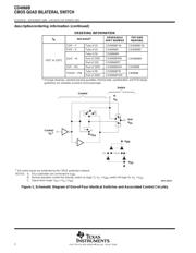
description/ordering information
The CD4066B is a quad bilateral switch intended for the transmission or multiplexing of analog or digital signals.
It is pin-for-pin compatible with the CD4016B, but exhibits a much lower on-state resistance. In addition, the
on-state resistance is relatively constant over the full signal-input range.
The CD4066B consists of four bilateral switches, each with independent controls. Both the p and the n devices
in a given switch are biased on or off simultaneously by the control signal. As shown in Figure 1, the well of the
n-channel device on each switch is tied to either the input (when the switch is on) or to V
SS
(when the switch
is off). This configuration eliminates the variation of the switch-transistor threshold voltage with input signal and,
thus, keeps the on-state resistance low over the full operating-signal range.
The advantages over single-channel switches include peak input-signal voltage swings equal to the full supply
voltage and more constant on-state impedance over the input-signal range. However, for sample-and-hold
applications, the CD4016B is recommended.
Copyright 2003, Texas Instruments Incorporated
!" #!$% &"'
&! #" #" (" " ") !"
&& *+' &! #", &" ""%+ %!&"
", %% #""'
Please be aware that an important notice concerning availability, standard warranty, and use in critical applications of
Texas Instruments semiconductor products and disclaimers thereto appears at the end of this data sheet.
1
2
3
4
5
6
7
14
13
12
11
10
9
8
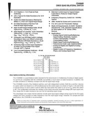
SIG A IN/OUT
SIG A OUT/IN
SIG B OUT/IN
SIG B IN/OUT
CONTROL B
CONTROL C
V
SS
V
DD
CONTROL A
CONTROL D
SIG D IN/OUT
SIG D OUT/IN
SIG C OUT/IN
SIG C IN/OUT
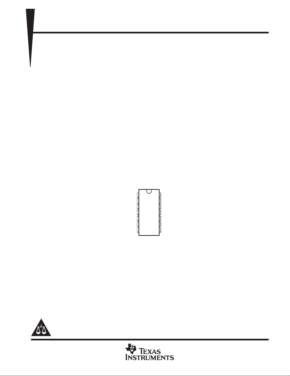
E, F, M, NS, OR PW PACKAGE
(TOP VIEW)
器件 Datasheet 文档搜索
AiEMA 数据库涵盖高达 72,405,303 个元件的数据手册,每天更新 5,000 多个 PDF 文件
