Datasheet 搜索 > 多工器 > TI(德州仪器) > CD74HC4052PWR 数据手册 > CD74HC4052PWR 数据手册 1/45 页

 器件3D模型
¥ 0.755
CD74HC4052PWR 数据手册 - TI(德州仪器)
制造商:
TI(德州仪器)
分类:
多工器
封装:
TSSOP-16
描述:
TEXAS INSTRUMENTS CD74HC4052PWR 芯片, 模拟多路复用器/信号分离器, 双路, 4:1, TSSOP-16
Pictures:
3D模型
符号图
焊盘图
引脚图
产品图
页面导航:
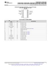
引脚图在P3P4P5Hot
典型应用电路图在P1P23P24
原理图在P20P21
封装尺寸在P28P29P30P31P32P33P35P36P37
标记信息在P28P29P30P31P32P33
封装信息在P27P28P29P30P31P32P33P34P35P36P37
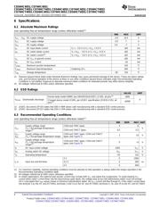
技术参数、封装参数在P6P16P24
应用领域在P1P34P45
电气规格在P6P7P8P9P10P11P24
导航目录
CD74HC4052PWR数据手册
Page:
of 45 Go
若手册格式错乱,请下载阅览PDF原文件
TG
TG
TG
TG
TG
TG
TG
3
A
COMMO
N
OUT/IN
BINARY
TO
1 OF 8
DECODER
WITH
ENABLE
11
10
9
6E
S
2
S
1
S
0
LOGIC
LEVEL
CONVERSION
8 7
GND V
EE
16
V
CC
131415121524
A A A A A A A A
7 6 5 4 3 2 1 0
CHANNEL IN/OUT
TG
Product
Folder
Sample &
Buy
Technical
Documents
Tools &
Software
Support &
Community
CD54HC4051
,
CD74HC4051
CD54HCT4051
,
CD74HCT4051
,
CD54HC4052
,
CD74HC4052
,
CD54HCT4052
CD74HCT4052
,
CD54HC4053
,
CD74HC4053
,
CD54HCT4053
,
CD74HCT4053
SCHS122K –NOVEMBER 1997–REVISED SEPTEMBER 2015
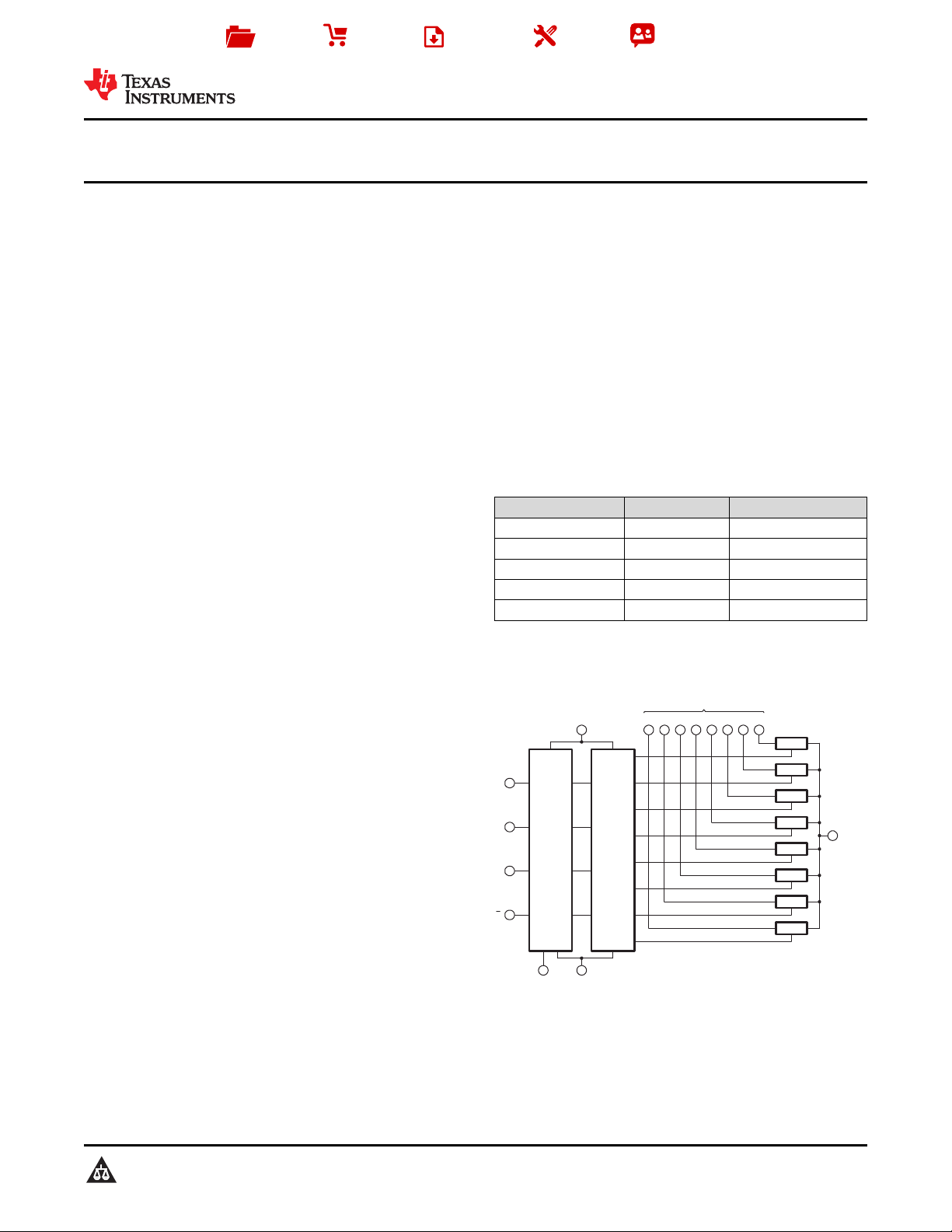
CDx4HC405x, CDx4HCT405x High-Speed CMOS Logic Analog
Multiplexers and Demultiplexers
1 Features 3 Description
The CDx4HC405x and CDx4HCT405x devices are
1
• Wide Analog Input Voltage Range: ±5-V Maximum
digitally controlled analog switches that use silicon
• Low ON-Resistance
gate CMOS technology to achieve operating speeds
– 7-Ω Typical (V
CC
– V
EE
= 4.5 V)
similar to LSTTL with the low-power consumption of
standard CMOS integrated circuits.
– 40-Ω Typical (V
CC
– V
EE
= 9 V)
• Low Crosstalk Between Switches
These analog multiplexers and demultiplexers control
analog voltages that may vary across the voltage
• Fast Switching and Propagation Speeds
supply range (for example, V
CC
to V
EE
). They are
• Break-Before-Make Switching
bidirectional switches that allow any analog input to
• Wide Operating Temperature Range:
be used as an output and vice versa. The switches
–55°C to +125°C
have low ON resistance and low OFF leakages. In
addition, all these devices have an enable control
• CD54HC and CD74HC Types
that, when high, disables all switches to their OFF
– Operation Control Voltage: 2 V to 6 V
state.
– Switch Voltage: 0 V to 10 V
Device Information
(1)
• CD54HCT and CD74HCT Types
PART NUMBER PACKAGE BODY SIZE (NOM)
– Operation Control Voltage: 4.5 V to 5.5 V
CD54HCx405xF CDIP (16) 19.56 mm × 6.92 mm
– Switch Voltage: 0 V to 10 V
CD74HCx405xE PDIP (16) 19.30 mm × 6.35 mm
– Direct LSTTL Input Logic Compatibility
CD74HCx405xM SOIC (16) 9.90 mm × 3.91 mm
V
IL
= 0.8-V Max, V
IH
= 2-V Min
CD74HCx405xNS SOP (16) 10.30 mm × 5.30 mm
– CMOS Input Compatibility
CD74HCx405xPW TSSOP (16) 5.00 mm × 4.40 mm
I
I
≤ 1 µA at V
OL
, V
OH
(1) For all available packages, see the orderable addendum at
• On Products Compliant to MIL-PRF-38535,
the end of the data sheet.
All Parameters Are Tested Unless Otherwise
Noted. On All Other Products, Production
Functional Diagram of HC4051 and HCT4051
Processing Does Not Necessarily Include Testing
of All Parameters.
2 Applications
• Digital Radio
• Signal Gating
• Factory Automation
• Televisions
• Appliances
• Programmable Logic Circuits
• Sensors
1
An IMPORTANT NOTICE at the end of this data sheet addresses availability, warranty, changes, use in safety-critical applications,
intellectual property matters and other important disclaimers. PRODUCTION DATA.
器件 Datasheet 文档搜索
AiEMA 数据库涵盖高达 72,405,303 个元件的数据手册,每天更新 5,000 多个 PDF 文件
