Datasheet 搜索 > 多工器 > TI(德州仪器) > CD74HC4052PWR 数据手册 > CD74HC4052PWR 数据手册 6/45 页

 器件3D模型
¥ 0.758
CD74HC4052PWR 数据手册 - TI(德州仪器)
制造商:
TI(德州仪器)
分类:
多工器
封装:
TSSOP-16
描述:
TEXAS INSTRUMENTS CD74HC4052PWR 芯片, 模拟多路复用器/信号分离器, 双路, 4:1, TSSOP-16
Pictures:
3D模型
符号图
焊盘图
引脚图
产品图
页面导航:
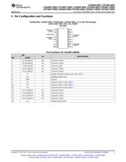
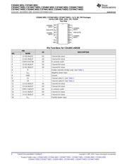
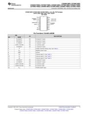
引脚图在P3P4P5Hot
典型应用电路图在P1P23P24
原理图在P20P21
封装尺寸在P28P29P30P31P32P33P35P36P37
标记信息在P28P29P30P31P32P33
封装信息在P27P28P29P30P31P32P33P34P35P36P37
技术参数、封装参数在P6P16P24
应用领域在P1P34P45
电气规格在P6P7P8P9P10P11P24
导航目录
CD74HC4052PWR数据手册
Page:
of 45 Go
若手册格式错乱,请下载阅览PDF原文件
CD54HC4051
,
CD74HC4051
CD54HCT4051
,
CD74HCT4051
,
CD54HC4052
,
CD74HC4052
,
CD54HCT4052
CD74HCT4052
,
CD54HC4053
,
CD74HC4053
,
CD54HCT4053
,
CD74HCT4053
SCHS122K –NOVEMBER 1997–REVISED SEPTEMBER 2015
www.ti.com
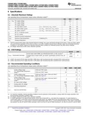
6 Specifications
6.1 Absolute Maximum Ratings
over operating free-air temperature range (unless otherwise noted)
(1)
MIN MAX UNIT
V
CC
– V
EE
DC supply voltage –0.5 10.5 V
V
CC
DC supply voltage –0.5 7 V
V
EE
DC supply voltage 0.5 –7 V
I
IK
DC input diode current V
I
< – 0.5 V or V
I
> V
CC
+ 0.5 V ±20 mA
I
OK
DC switch diode current V
I
< V
EE
– 0.5 V or V
I
> V
CC
+ 0.5 V ±20 mA
DC switch current
(2)
V
I
> V
EE
– 0.5 V or V
I
< V
CC
+ 0.5 V ±25 mA
I
CC
DC V
CC
or ground current ±50 mA
I
EE
DC V
EE
current –20 mA
T
JMAX
Maximum junction temperature 150 °C
T
LMAX
Maximum lead temperature Soldering 10 s 300 °C
T
stg
Storage temperature –65 150 °C
(1) Stresses beyond those listed under Absolute Maximum Ratings may cause permanent damage to the device. These are stress ratings
only, and functional operation of the device at these or any other conditions beyond those indicated under Recommended Operating
Conditions is not implied. Exposure to absolute-maximum-rated conditions for extended periods may affect device reliability.
(2) All voltages referenced to GND unless otherwise specified.
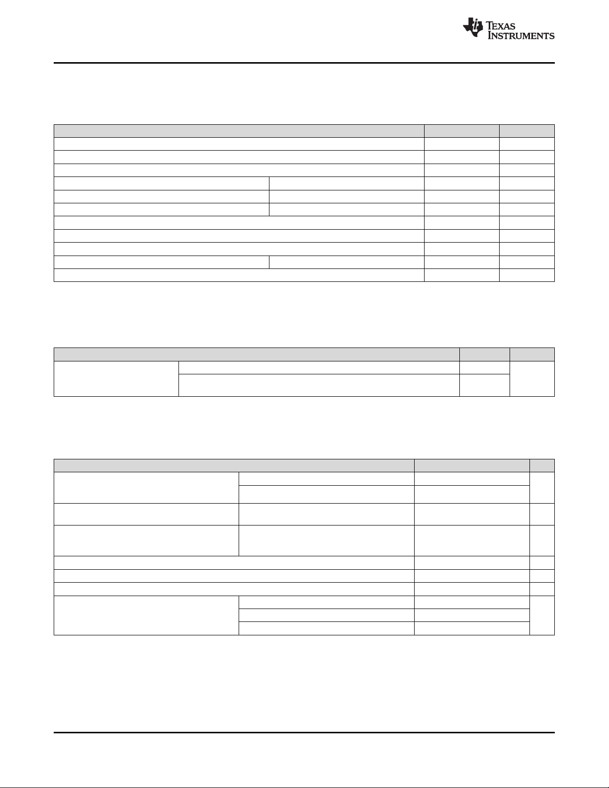
6.2 ESD Ratings
VALUE UNIT
Human body model (HBM), per ANSI/ESDA/JEDEC JS-001, all pins
(1)
±500
V
(ESD)
Electrostatic discharge V
Charged device model (CDM), per JEDEC specification JESD22-C101, all
±1000
pins
(2)
(1) JEDEC document JEP155 states that 500-V HBM allows safe manufacturing with a standard ESD control process.
(2) JEDEC document JEP157 states that 250-V CDM allows safe manufacturing with a standard ESD control process.
6.3 Recommended Operating Conditions
over operating free-air temperature range (unless otherwise noted)
(1)
MIN NOM MAX UNIT
Supply voltage range CD54 and 74HC types 2 6
V
CC
(T
A
= full package temperature V
CD54 and 74HCT types 4.5 5.5
range)
(2)
V
CC
– Supply voltage range CD54 and 74HC types, CD54 and 74HCT
2 10 V
V
EE
(T
A
= full package temperature range) types (see Figure 1)
Supply voltage range
CD54 and 74HC types, CD54 and 74HCT
V
EE
(T
A
= full package temperature 0 –6 V
types (see Figure 2)
range)
(3)
V
I
DC input control voltage GND V
CC
V
V
IS
Analog switch I/O voltage V
EE
V
CC
V
T
A
Operating temperature –55 125 °C
2 V 0 1000
t
r
, t
f
Input rise and fall times 4.5 V 0 500 ns
6 V 0 400
(1) For maximum reliability, nominal operating conditions must be selected so that operation is always within the ranges specified in the
Recommended Operating Conditions table.
(2) All voltages referenced to GND unless otherwise specified.
(3) In certain applications, the external load resistor current may include both V
CC
and signal line components. To avoid drawing V
CC
current when switch current flows into the transmission gate inputs, the voltage drop across the bidirectional switch must not exceed
0.6 V (calculated from r
ON
values shown in Electrical Specifications table). No V
CC
current will flow through R
L
if the switch current flows
into terminal 3 on the HC and HCT4051; terminals 3 and 13 on the HC and HCT4052; terminals 4, 14, and 15 on the HC and HCT4053.
6 Submit Documentation Feedback Copyright © 1997–2015, Texas Instruments Incorporated
Product Folder Links: CD54HC4051 CD74HC4051 CD54HCT4051 CD74HCT4051 CD54HC4052 CD74HC4052
CD54HCT4052 CD74HCT4052 CD54HC4053 CD74HC4053 CD54HCT4053 CD74HCT4053
器件 Datasheet 文档搜索
AiEMA 数据库涵盖高达 72,405,303 个元件的数据手册,每天更新 5,000 多个 PDF 文件
