Datasheet 搜索 > 逻辑控制器 > TI(德州仪器) > CD74HCT166M96 数据手册 > CD74HCT166M96 数据手册 1/16 页
 器件3D模型
¥ 1.895
CD74HCT166M96 数据手册 - TI(德州仪器)
制造商:
TI(德州仪器)
分类:
逻辑控制器
封装:
SOIC-16
描述:
高速CMOS逻辑8位并行输入/串行输出移位寄存器 High-Speed CMOS Logic 8-Bit Parallel-In/Serial-Out Shift Register
Pictures:
3D模型
符号图
焊盘图
引脚图
产品图
页面导航:
导航目录
CD74HCT166M96数据手册
Page:
of 16 Go
若手册格式错乱,请下载阅览PDF原文件
1
Data sheet acquired from Harris Semiconductor
SCHS157C
Features
• Buffered Inputs
• Fanout (Over Temperature Range)
- Standard Outputs. . . . . . . . . . . . . . . 10 LSTTL Loads
- Bus Driver Outputs . . . . . . . . . . . . . 15 LSTTL Loads
• Wide Operating Temperature Range . . . -55
o
C to 125
o
C
• Balanced Propagation Delay and Transition Times
• Significant Power Reduction Compared to LSTTL
Logic ICs
• HC Types
- 2V to 6V Operation
- High Noise Immunity: N
IL
= 30%, N
IH
= 30% of V
CC
at V
CC
= 5V
• HCT Types
- 4.5V to 5.5V Operation
- Direct LSTTL Input Logic Compatibility,
V
IL
= 0.8V (Max), V
IH
= 2V (Min)
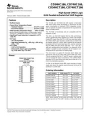
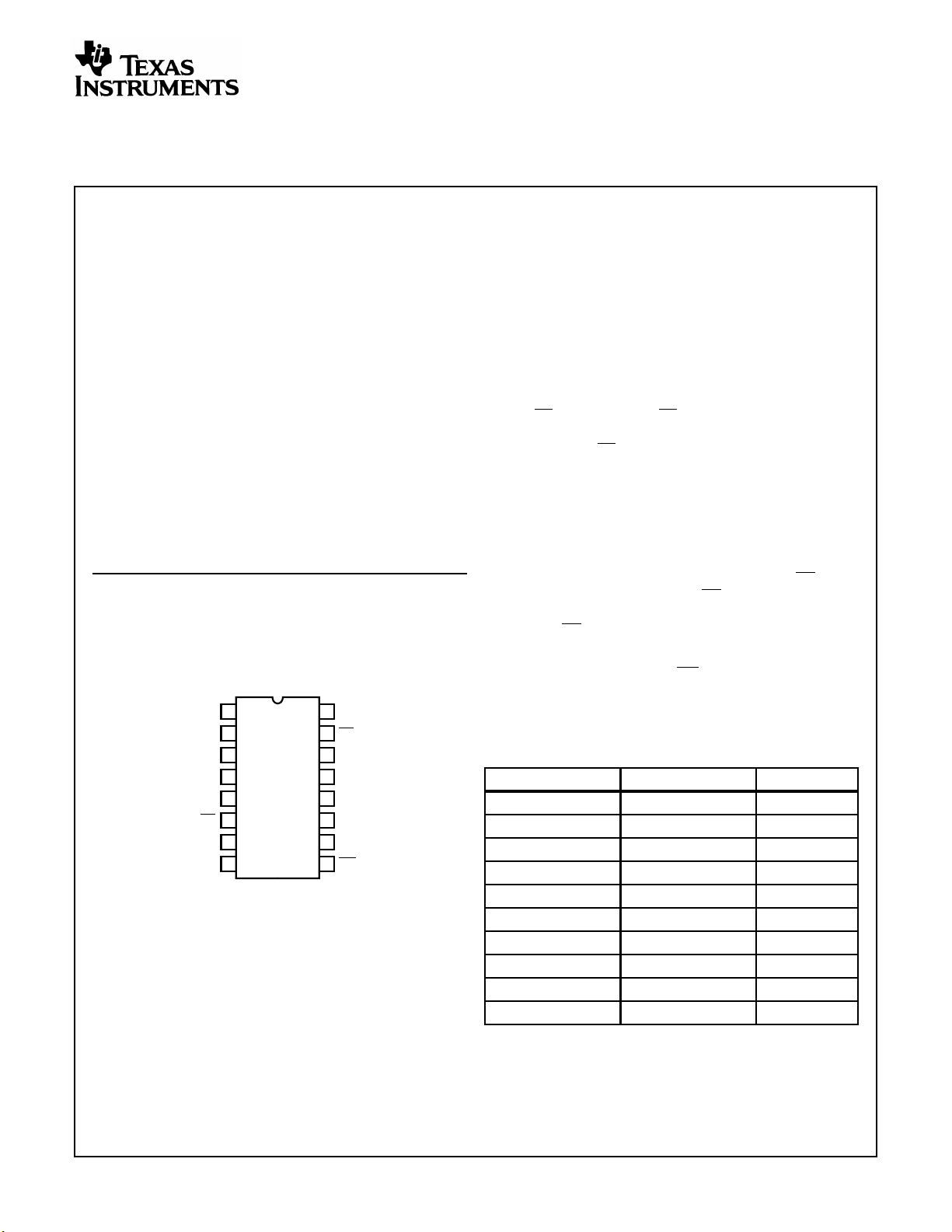
Pinout
CD54HC166, CD54HCT166
(CERDIP)
CD74HC166, CD74HCT166
(PDIP, SOIC)
TOP VIEW
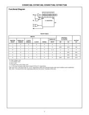
Description
The ’HC166 and ’HCT166 8-bit shift register is fabricated
with silicon gate CMOS technology. It possesses the low
power consumption of standard CMOS integrated circuits,
and can operate at speeds comparable to the equivalent low
power Schottky device.
The ’HCT166 is functionally and pin compatible with the
standard ’LS166.
The 166 is an 8-bit shift register that has fully synchronous
serial or parallel data entry selected by an active LOW Parallel
Enable (
PE) input. When the PE is LOW one setup time before
the LOW-to-HIGH clock transition, parallel data is entered into
the register. When
PE is HIGH, data is entered into the internal
bit position Q0 from Serial Data Input (DS), and the remaining
bits are shifted one place to the right (Q0 → Q1 → Q2, etc.)
with each positive-going clock transition. For expansion of the
register in parallel to serial converters, the Q7 output is con-
nected to the DS input of the succeeding stage.
The clock input is a gated OR structure which allows one
input to be used as an active LOW Clock Enable (
CE) input.
The pin assignment for the CP and
CE inputs is arbitrary and
can be reversed for layout convenience. The LOW-to-HIGH
transition of
CE input should only take place while the CP is
HIGH for predictable operation.
A LOW on the Master Reset (
MR) input overrides all other
inputs and clears the register asynchronously, forcing all bit
positions to a LOW state.
Ordering Information
14
15
16
9
13
12
11
10
1
2
3
4
5
7
6
8
DS
D0
D1
D2
D3
CE
GND
CP
V
CC
D7
Q7
D6
D5
D4
MR
PE
PART NUMBER TEMP. RANGE (
o
C) PACKAGE
CD54HC166F3A -55 to 125 16 Ld CERDIP
CD54HCT166F3A -55 to 125 16 Ld CERDIP
CD74HC166E -55 to 125 16 Ld PDIP
CD74HC166M -55 to 125 16 Ld SOIC
CD74HC166MT -55 to 125 16 Ld SOIC
CD74HC166M96 -55 to 125 16 Ld SOIC
CD74HCT166E -55 to 125 16 Ld PDIP
CD74HCT166M -55 to 125 16 Ld SOIC
CD74HCT166MT -55 to 125 16 Ld SOIC
CD74HCT166M96 -55 to 125 16 Ld SOIC
NOTE: When ordering, use the entire part number. The suffix 96
denotes tape and reel. The suffix T denotes a small-quantity reel of
250.
February 1998 - Revised October 2003
CAUTION: These devices are sensitive to electrostatic discharge. Users should follow proper IC Handling Procedures.
Copyright
© 2003, Texas Instruments Incorporated
CD54HC166, CD74HC166,
CD54HCT166, CD74HCT166
High-Speed CMOS Logic
8-Bit Parallel-In/Serial-Out Shift Register
[
/Title
(
CD74
H
C166
,
C
D74
H
CT16
6
)
/
Sub-
j
ect
(
High
S
peed
C
MOS
L
ogic
8
-Bit
P
aral-
l
el-
I
n/Seri
器件 Datasheet 文档搜索
AiEMA 数据库涵盖高达 72,405,303 个元件的数据手册,每天更新 5,000 多个 PDF 文件
