Datasheet 搜索 > MOS管 > TI(德州仪器) > CSD87350Q5D 数据手册 > CSD87350Q5D 数据手册 5/23 页

¥ 3.812
CSD87350Q5D 数据手册 - TI(德州仪器)
制造商:
TI(德州仪器)
分类:
MOS管
封装:
LSON-CLIP-8
描述:
同步降压 NexFET™ 电源块 MOSFET 对
Pictures:
3D模型
符号图
焊盘图
引脚图
产品图
页面导航:
导航目录
CSD87350Q5D数据手册
Page:
of 23 Go
若手册格式错乱,请下载阅览PDF原文件
Board Temperature (qC)
Output Current (A)
0 20 40 60 80 100 120 140
0
5
10
15
20
25
30
35
40
45
D006
Switching Frequency (kHz)
Power Loss, Normalized
SOA Temperature Adj. (qC)
200 400 600 800 1000 1200 1400 1600
0.9 -2.9
1 0.0
1.1 2.9
1.2 5.9
1.3 8.8
1.4 11.8
1.5 14.7
D007
Ambient Temperature (qC)
Output Current (A)
0 10 20 30 40 50 60 70 80 90
0
5
10
15
20
25
30
35
40
45
D004
400 LFM
200 LFM
100 LFM
Nat. conv.
Ambient Temperature (qC)
Output Current (A)
0 10 20 30 40 50 60 70 80 90
0
5
10
15
20
25
30
35
40
45
D005
400 LFM
200 LFM
100 LFM
Nat. conv.
Output Current (A)
Power Loss (W)
0 5 10 15 20 25 30 35 40
0
1
2
3
4
5
6
7
8
9
10
D002
T
C
- Junction Temperature (qC)
Power Loss, Normalized
-50 -30 -10 10 30 50 70 90 110 130 150
0.65
0.7
0.75
0.8
0.85
0.9
0.95
1
1.05
D003
CSD87350Q5D
www.ti.com
SLPS288D –MARCH 2011–REVISED SEPTEMBER 2014
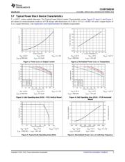
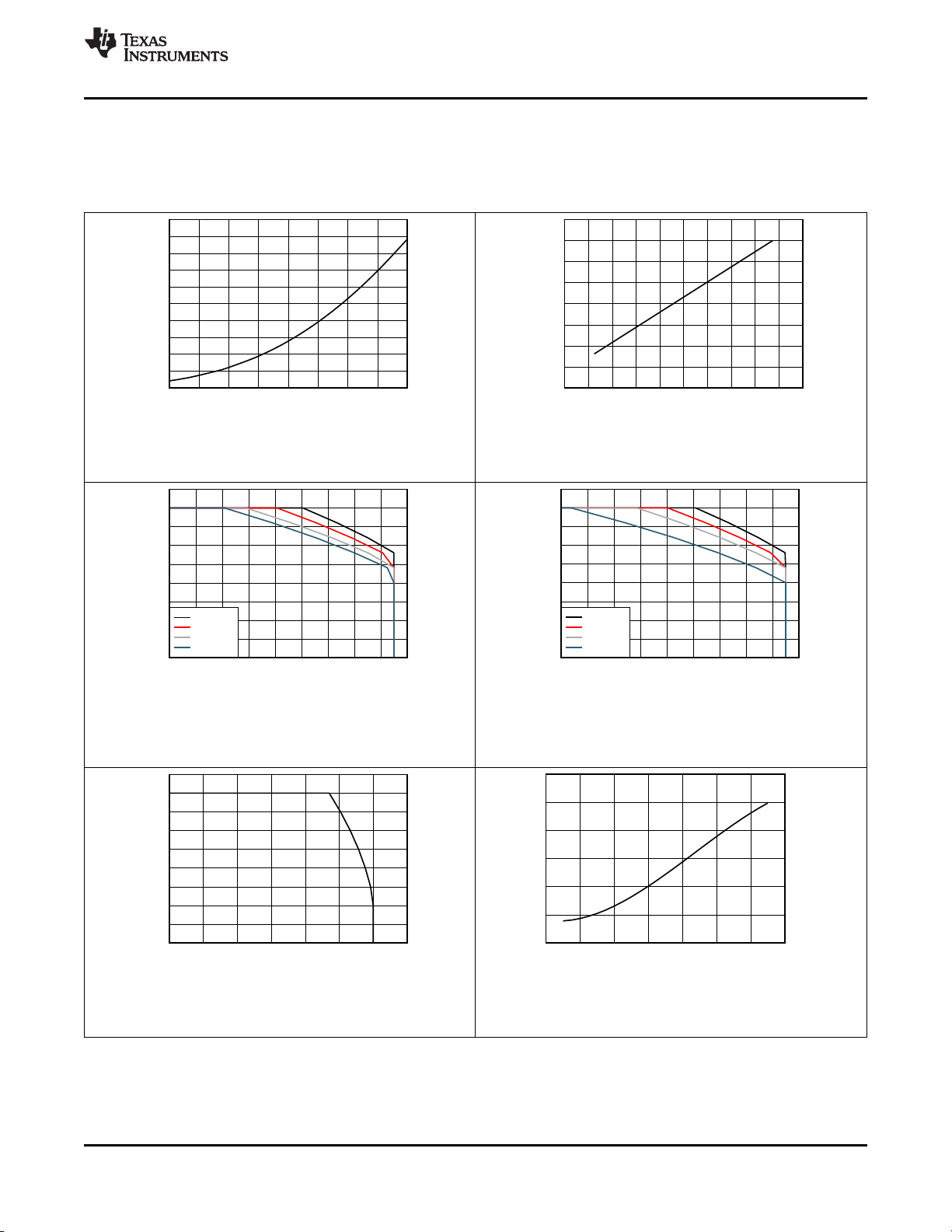
5.7 Typical Power Block Device Characteristics
T
J
= 125°C, unless stated otherwise. The Typical Power Block System Characteristic curves Figure 3, Figure 4, and Figure 5
are based on measurements made on a PCB design with dimensions of 4” (W) × 3.5” (L) × 0.062” (H) and 6 copper layers of
1 oz. copper thickness. See Application and Implementation for detailed explanation.
V
IN
= 12 V V
GS
= 5 V V
OUT
= 1.3 V V
IN
= 12 V V
GS
= 5 V V
OUT
= 1.3 V
ƒ
SW
= 500 kHz L
OUT
= 0.3 µH ƒ
SW
= 500 kHz L
OUT
= 0.3 µH
Figure 1. Power Loss vs Output Current Figure 2. Normalized Power Loss vs Temperature
V
IN
= 12 V V
GS
= 5 V V
OUT
= 1.3 V V
IN
= 12 V V
GS
= 5 V V
OUT
= 1.3 V
ƒ
SW
= 500 kHz L
OUT
= 0.3 µH ƒ
SW
= 500 kHz L
OUT
= 0.3 µH
Figure 3. Safe Operating Area (SOA) – PCB Vertical Mount Figure 4. Safe Operating Area (SOA) – PCB Horizontal
Mount
V
IN
= 12 V V
GS
= 5 V V
OUT
= 1.3 V V
IN
= 12 V V
GS
= 5 V V
OUT
= 1.3 V
ƒ
SW
= 500 kHz L
OUT
= 0.3 µH L
OUT
= 0.3 µH I
OUT
= 40 A
Figure 5. Typical Safe Operating Area (SOA) Figure 6. Normalized Power Loss vs Switching Frequency
Copyright © 2011–2014, Texas Instruments Incorporated Submit Documentation Feedback 5
器件 Datasheet 文档搜索
AiEMA 数据库涵盖高达 72,405,303 个元件的数据手册,每天更新 5,000 多个 PDF 文件
