Datasheet 搜索 > TI(德州仪器) > DAC5687 数据手册 > DAC5687 数据手册 31/79 页

 器件3D模型
¥ 0
DAC5687 数据手册 - TI(德州仪器)
制造商:
TI(德州仪器)
封装:
HTQFP-100
描述:
16 位 500 MSPS 2x-8x 内插双通道数模转换器 (DAC)
Pictures:
3D模型
符号图
焊盘图
引脚图
产品图
页面导航:
引脚图在P33Hot
典型应用电路图在P65
原理图在P2P20P21P22P23P36P39P51P65
封装尺寸在P74P75P76
焊盘布局在P65
型号编码规则在P1
封装信息在P74P75P76
技术参数、封装参数在P5P6P7P8P9P10P20
应用领域在P1P74P79
电气规格在P6P7P8P9P10P20
导航目录
DAC5687数据手册
Page:
of 79 Go
若手册格式错乱,请下载阅览PDF原文件
www.ti.com
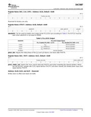
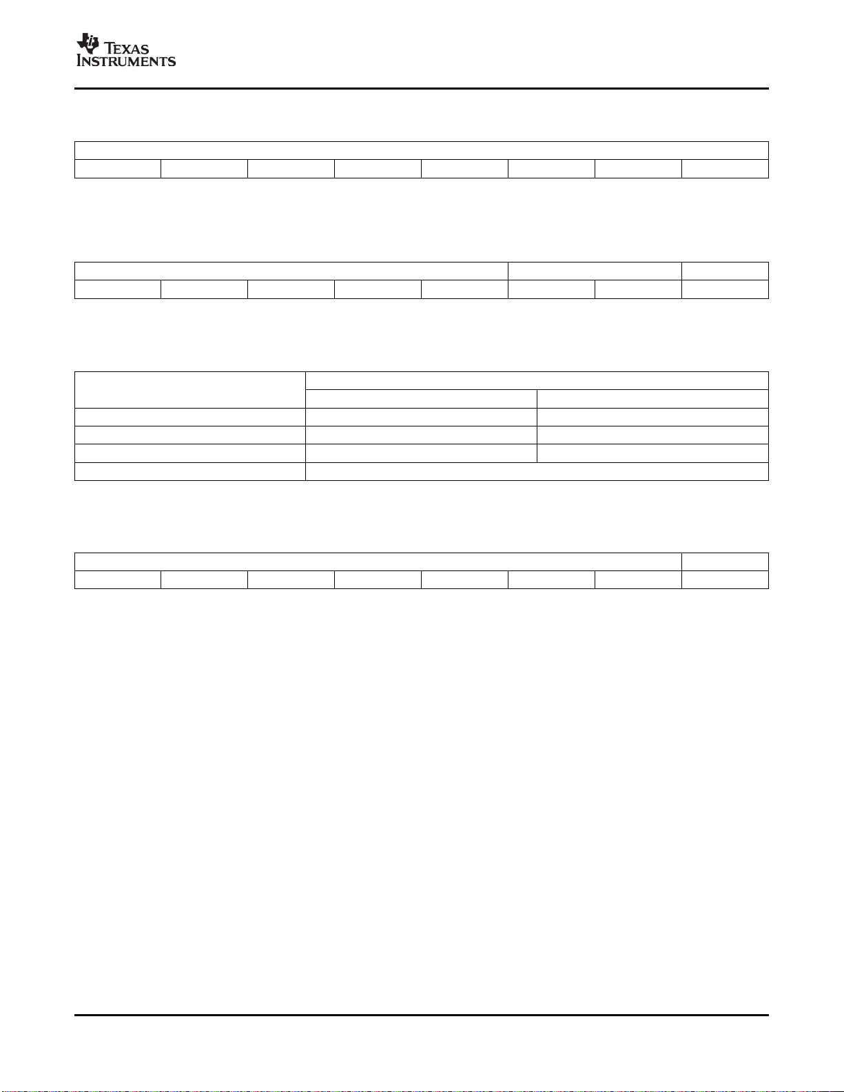
Register Name: DAC_CLK_CNTL — Address: 0x1A, Default = 0x00
Register Name: ATEST — Address: 0x1B, Default = 0x00
Register Name: DAC_TEST — Address: 0x1C, Default = 0x00
Address: 0x1D, 0x1E, and 0x1F – Reserved
DAC5687
SLWS164E – FEBRUARY 2005 – REVISED SEPTEMBER 2006
BIT 7 BIT 0
Factory use only
0 0 0 0 0 0 0 0
Reserved for factory use only.
BIT 7 BIT 0
atest(4:0) phstr_del(1:0) unused
0 0 0 0 0 0 0 0
atest(4:0): Can be used to enable clock output at the PLLLOCK pin according to Table 5 . Pin EXTLO must be
open when atest(4:0) is not equal to 00000.
Table 5. PLLLOCK Output
atest(4:0) PLLLOCK Output Signal
PLL Enabled (PLLVDD = 3.3 V) PLL Disabled (PLLVDD = 0 V)
11101 f
DAC
Normal operation
11110 f
DAC
divided by 2 Normal operation
11111 f
DAC
divided by 4 Normal operation
All others Normal operation
phstr_del: Adjusts the initial phase of the f
S
/2 and f
S
/4 blocks cmix block after PHSTR.
BIT 7 BIT 0
Factory use only phstr_clkdiv_sel
0 0 0 0 0 0 0 0
phstr_clkdiv_sel: Selects the clock used to latch the PHSTR input when restarting the internal dividers. When
set, the full DAC sample rate CLK2 signal latches PHSTR, and when cleared, the divided down input clock
signal latches PHSTR.
Writes have no effect and reads are 0x00.
Copyright © 2005 – 2006, Texas Instruments Incorporated Submit Documentation Feedback 31
Product Folder Link(s): DAC5687
器件 Datasheet 文档搜索
AiEMA 数据库涵盖高达 72,405,303 个元件的数据手册,每天更新 5,000 多个 PDF 文件
