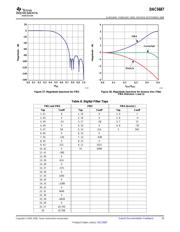
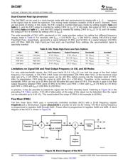
Datasheet 搜索 > TI(德州仪器) > DAC5687 数据手册 > DAC5687 数据手册 33/79 页

 器件3D模型
¥ 0
DAC5687 数据手册 - TI(德州仪器)
制造商:
TI(德州仪器)
封装:
HTQFP-100
描述:
16 位 500 MSPS 2x-8x 内插双通道数模转换器 (DAC)
Pictures:
3D模型
符号图
焊盘图
引脚图
产品图
页面导航:
引脚图在P33Hot
典型应用电路图在P65
原理图在P2P20P21P22P23P36P39P51P65
封装尺寸在P74P75P76
焊盘布局在P65
型号编码规则在P1
封装信息在P74P75P76
技术参数、封装参数在P5P6P7P8P9P10P20
应用领域在P1P74P79
电气规格在P6P7P8P9P10P20
导航目录
DAC5687数据手册
Page:
of 79 Go
若手册格式错乱,请下载阅览PDF原文件
www.ti.com
R/W
t
(SCLKL)
SDENB
SCLK
SDIO N1 N0 A3 A2 A1 A0 D7 D6 D5 D4 D3 D2 D1 D0
SDENB
SCLK
SDIO
Instruction Cycle Data Transfer Cycle(s)
t
s(SDENB)
t
(SCLK)
t
h(SDIO)
t
s(SDIO)
t
(SCLKH)
T0037-02
A4
R/W
D7
SDENB
SCLK
SDIO N1 N0 A4 A3 A2 A1 A0 D6 D5 D4 D3 D2 D0 0
Instruction Cycle
Data Transfer Cycle(s)
SDO D7 D6 D5 D4 D3 D2 D1 D0
0
3-Pin Configuration
Output
4-Pin Configuration
Output
SDENB
SCLK
SDIO
Data n Data n−1
SDO
t
d(DATA)
D1
T0038-02
DAC5687
SLWS164E – FEBRUARY 2005 – REVISED SEPTEMBER 2006
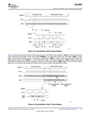
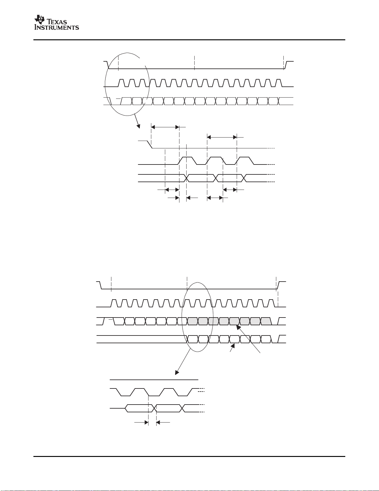
Figure 33. Serial-Interface Write Timing Diagram
Figure 34 shows the serial interface timing diagram for a DAC5687 read operation. SCLK is the serial interface
clock input to the DAC5687. Serial data enable SDENB is an active-low input to the DAC5687. SDIO is serial
data in during the instruction cycle. In three-pin configuration, SDIO is data out from the DAC5687 during the
data transfer cycle(s), while SDO is in a high-impedance state. In four-pin configuration, SDO is data out from the
DAC5687 during the data transfer cycle(s). At the end of the data transfer, SDO outputs low on the final falling
edge of SCLK until the rising edge of SDENB, when it goes into the high-impedance state.
Figure 34. Serial-Interface Read Timing Diagram
Copyright © 2005 – 2006, Texas Instruments Incorporated Submit Documentation Feedback 33
Product Folder Link(s): DAC5687
器件 Datasheet 文档搜索
AiEMA 数据库涵盖高达 72,405,303 个元件的数据手册,每天更新 5,000 多个 PDF 文件
