Datasheet 搜索 > 接口芯片 > TI(德州仪器) > DS90C387AVJD/NOPB 数据手册 > DS90C387AVJD/NOPB 数据手册 2/21 页
 器件3D模型
¥ 43.109
DS90C387AVJD/NOPB 数据手册 - TI(德州仪器)
制造商:
TI(德州仪器)
分类:
接口芯片
封装:
TQFP-100
描述:
FlatLink/FPD-Link(LVDS,用于 LCD),Texas InstrumentsLVDS 发射器适合与以 65 和 85 MHz 工作的 24位 FPD(平板显示屏)链路一起工作。LVCMOS/LVTTL 输入 3.3V 低功耗工作 PLL 发射器数据时钟 符合 TIA/EIA-644 LVDS 标准 ### LVDS 通信低压差分信号或 LVDS 是可以在廉价双绞线铜电缆上以极高速度运行的电子信号系统。应用:Firewire、SATA、SCSI
Pictures:
3D模型
符号图
焊盘图
引脚图
产品图
页面导航:
导航目录
DS90C387AVJD/NOPB数据手册
Page:
of 21 Go
若手册格式错乱,请下载阅览PDF原文件
DS90C387A/DS90CF388A
Dual Pixel LVDS Display Interface / FPD-Link
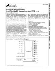
General Description
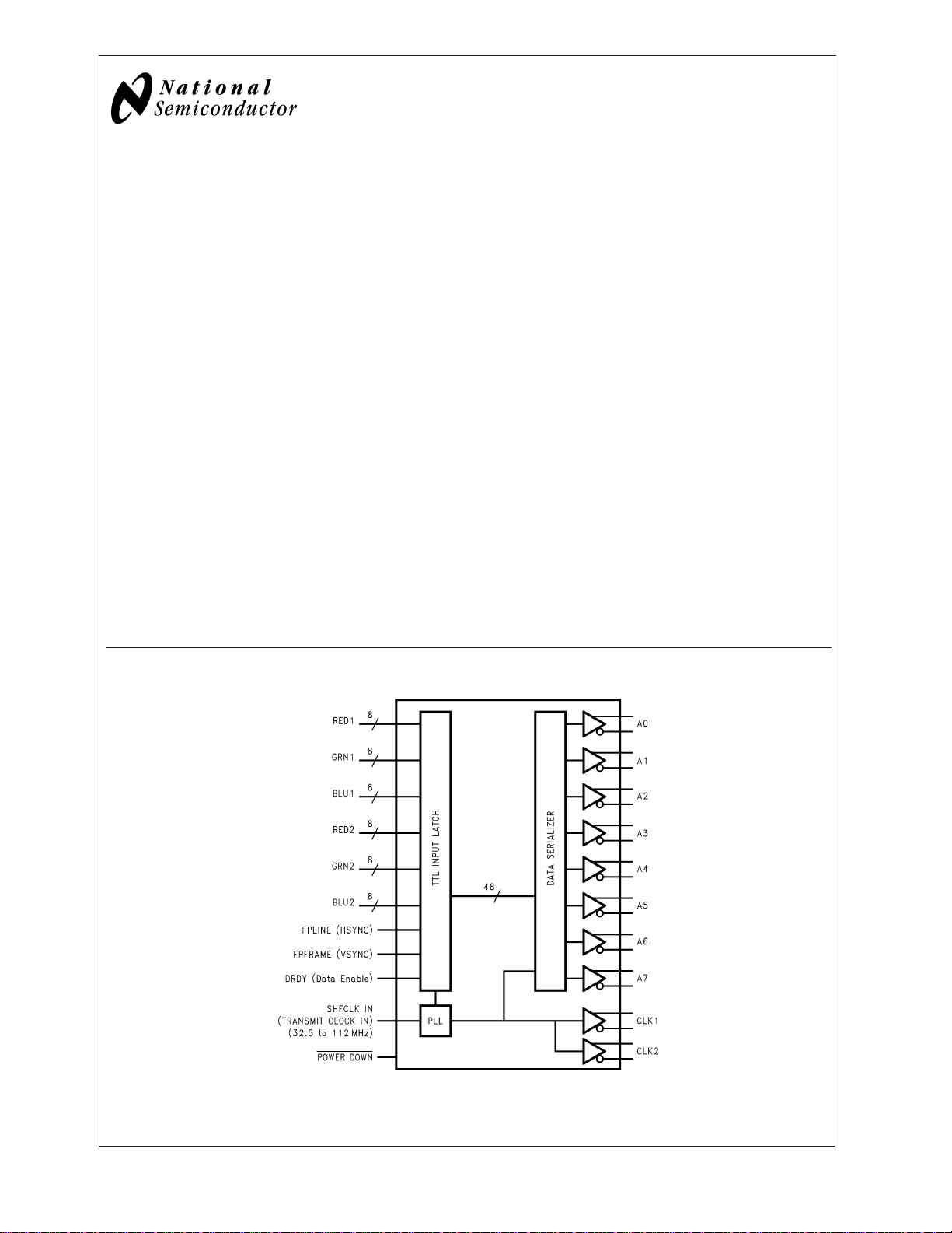
The DS90C387A/DS90CF388A transmitter/receiver pair is
designed to support dual pixel data transmission between
Host and Flat Panel Display up to QXGA resolutions. The
transmitter converts 48 bits (Dual Pixel 24-bit color) of
CMOS/TTL data and 3 control bits into 8 LVDS (Low Voltage
Differential Signalling) data streams. At a maximum dual
pixel rate of 112MHz, LVDS data line speed is 784Mbps,
providing a total throughput of 5.7Gbps (714 Megabytes per
second).
The LDI chipset is improved over prior generations of FPD-
Link devices and offers higher bandwidth support and longer
cable drive. To increase bandwidth, the maximum pixel clock
rate is increased to 112 MHz and 8 serialized LVDS outputs
are provided. Cable drive is enhanced with a user selectable
pre-emphasis feature that provides additional output current
during transitions to counteract cable loading effects.
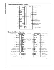
The DS90C387A transmitter provides a second LVDS output
clock. Both LVDS clocks are identical. This feature supports
backward compatibility with the previous generation of FPD-
Link Receivers - the second clock allows the transmitter to
interface to panels using a ’dual pixel’ configuration of two
24-bit or 18-bit FPD-Link receivers.
This chipset is an ideal means to solve EMI and cable size
problems for high-resolution flat panel applications. It pro-
vides a reliable interface based on LVDS technology that
delivers the bandwidth needed for high-resolution panels
while maximizing bit times, and keeping clock rates low to
reduce EMI and shielding requirements. For more details,
please refer to the “Applications Information” section of this
datasheet.
Features
n Supports SVGA through QXGA panel resolutions
n 32.5 to 112/170MHz clock support
n Drives long, low cost cables
n Up to 5.7 Gbps bandwidth
n Pre-emphasis reduces cable loading effects
n Dual pixel architecture supports interface to GUI and
timing controller; optional single pixel transmitter inputs
support single pixel GUI interface
n Transmitter rejects cycle-to-cycle jitter
n 5V tolerant on data and control input pins
n Programmable transmitter data and control strobe select
(rising or falling edge strobe)
n Backward compatible with FPD-Link
n Compatible with ANSI/TIA/EIA-644-1995 LVDS Standard
Generalized Transmitter Block Diagram
10132002
TRI-STATE
®
is a registered trademark of National Semiconductor Corporation.
February 2006
DS90C387A/DS90CF388A Dual Pixel LVDS Display Interface / FPD-Link
© 2006 National Semiconductor Corporation DS101320 www.national.com
器件 Datasheet 文档搜索
AiEMA 数据库涵盖高达 72,405,303 个元件的数据手册,每天更新 5,000 多个 PDF 文件
