Datasheet 搜索 > 接口芯片 > TI(德州仪器) > DS90C387RVJD/NOPB 数据手册 > DS90C387RVJD/NOPB 数据手册 1/32 页
 器件3D模型
¥ 75.204
DS90C387RVJD/NOPB 数据手册 - TI(德州仪器)
制造商:
TI(德州仪器)
分类:
接口芯片
封装:
TQFP-100
描述:
85MHz 双路 12 位双泵输入 LDI 发送器 VGA/UXGA 100-TQFP -10 to 70
Pictures:
3D模型
符号图
焊盘图
引脚图
产品图
页面导航:
导航目录
DS90C387RVJD/NOPB数据手册
Page:
of 32 Go
若手册格式错乱,请下载阅览PDF原文件
DS90C387R
www.ti.com
SNLS062G –NOVEMBER 2000–REVISED JANUARY 2014
DS90C387R 85MHz Dual 12-Bit Double Pumped Input LDI Transmitter - VGA/UXGA
Check for Samples: DS90C387R
1
FEATURES
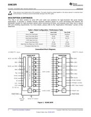
DESCRIPTION
The DS90C387R transmitter is designed to support
2
• Complies with Open LDI Specification for
pixel data transmission from a Host to a Flat Panel
Digital Display Interfaces
Display up to UXGA resolution. It is designed to be
• 25 to 85MHz Clock Support
compatible with Graphics Memory Controller Hub
• Supports VGA through UXGA Panel
(GMCH) by implementing two data per clock and can
be controlled by a two-wire serial communication
Resolution
interface. Two input modes are supported: one port of
• Up to 4.76Gbps Bandwidth in Dual 24-bit RGB
12-bit( two data per clock) input for 24-bit RGB, and
In-to-Dual Pixel Out Application
two ports of 12-bit( two data per clock) input for dual
• Dual 12-bit Double Pumped Input DVO Port
24-bit RGB( 48-bit total). In both modes, input data
will be clocked on both rising and falling edges in
• Pre-Emphasis Reduces Cable Loading Effects
LVTTL level operation, or clocked on the cross over
• Drives Long, Low Cost Cables
of differential clock signals in the low swing operation.
• DC Balance Data Transmission Provided by
Each input data width will be 1/2 of clock cycle. With
Transmitter Reduces ISI Distortion
an input clock at 85MHz and input data at 170Mbps,
the maximum transmission rate of each LVDS line is
• Transmitter Rejects Cycle-to-Cycle Jitter (±2ns
595Mbps, for a aggregate throughput rate of
of Input Bit Period)
2.38Gbps/4.76Gbps. It converts 24/48 bits
• Support both LVTTL and Low Voltage Level
(Single/Dual Pixel 24-bit color) of data into 4/8 LVDS
Input (Capable of 1.0 to 1.8V)
(Low Voltage Differential Signaling) data streams.
• Two-Wire Serial Communication Interface up
DS90C387R can be programmed via the two-wire
to 400 KHz
serial communication interface. The LVDS output pin-
out is identical to DS90C387. Thus, this transmitter
• Programmable Input Clock and Control Strobe
can be paired up with DS90CF388, receiver of the
Select
112MHz LDI chipset or FPD-Link Receivers in non-
• Backward Compatible Configuration with
DC Balance mode operation which provides GUI/LCD
112MHz LDI and FPD-Link
panel/mother board vendors a wide choice of inter-
operation with LVDS based TFT panels.
• Optional Second LVDS Clock for Backward
Compatibility with FPD-Link Receivers
DS90C387R also comes with features that can be
• Compatible with TIA/EIA-644
found on DS90C387. Cable drive is enhanced with a
user selectable pre-emphasis feature that provides
additional output current during transitions to
counteract cable loading effects. DC Balancing on a
cycle-to-cycle basis is also provided to reduce ISI
(Inter-Symbol Interference), control signals (VSYNC,
HSYNC, DE) are sent during blanking intervals. With
pre-emphasis and DC Balancing, a low distortion eye-
pattern is provided at the receiver end of the cable.
These enhancements allow cables 5 to 15+ meters in
length to be driven depending on media characteristic
and pixel clock speed. Pre-emphasis is available in
both the DC Balanced and Non-DC Balanced modes.
In the Non-DC Balanced mode backward
compatibility with FPD-Link Receivers is obtained.
1
Please be aware that an important notice concerning availability, standard warranty, and use in critical applications of
Texas Instruments semiconductor products and disclaimers thereto appears at the end of this data sheet.
2All trademarks are the property of their respective owners.
PRODUCTION DATA information is current as of publication date.
Copyright © 2000–2014, Texas Instruments Incorporated
Products conform to specifications per the terms of the Texas
Instruments standard warranty. Production processing does not
necessarily include testing of all parameters.
器件 Datasheet 文档搜索
AiEMA 数据库涵盖高达 72,405,303 个元件的数据手册,每天更新 5,000 多个 PDF 文件
