Datasheet 搜索 > 接口芯片 > TI(德州仪器) > DS90C387RVJD/NOPB 数据手册 > DS90C387RVJD/NOPB 数据手册 3/32 页
 器件3D模型
¥ 75.123
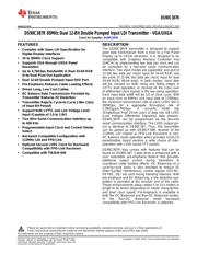
DS90C387RVJD/NOPB 数据手册 - TI(德州仪器)
制造商:
TI(德州仪器)
分类:
接口芯片
封装:
TQFP-100
描述:
85MHz 双路 12 位双泵输入 LDI 发送器 VGA/UXGA 100-TQFP -10 to 70
Pictures:
3D模型
符号图
焊盘图
引脚图
产品图
页面导航:
导航目录
DS90C387RVJD/NOPB数据手册
Page:
of 32 Go
若手册格式错乱,请下载阅览PDF原文件
DS90C387R
www.ti.com
SNLS062G –NOVEMBER 2000–REVISED JANUARY 2014
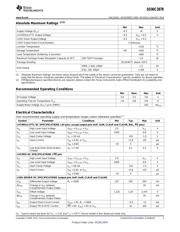
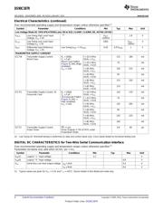
Absolute Maximum Ratings
(1)(2)
Min Max Unit
Supply Voltage (V
CC
) −0.3 +4 V
LVCMOS/LVTTL Output Voltage −0.3 V
CC
+ 0.3 V
LVDS Driver Output Voltage −0.3 V
CC
+ 0.3
LVDS Output Short Circuit Duration Continuous
Junction Temperature +150 °C
Storage Temperature −65 +150 °C
Lead Temperature (Soldering, 4 seconds) +260 °C
Maximum Package Power Dissipation Capacity at 25°C 100 TQFP Package 2.8 W
Package Derating 18.2mW/°C above +25°C
HBM, 1.5kΩ, 100pF > 2 kV
ESD Rating
EIAJ, 0Ω, 200pF > 300 V
(1) “Absolute Maximum Ratings” are those values beyond which the safety of the device cannot be guaranteed. They are not meant to
imply that the device should be operated at these limits. The tables of “Electrical Characteristics” specify conditions for device operation.
(2) If Military/Aerospace specified devices are required, please contact the Texas Instruments Sales Office/ Distributors for availability and
specifications.
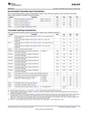
Recommended Operating Conditions
Min Nom Max Unit
All Supply Voltage 3.0 3.3 3.6 V
Operating Free Air Temperature (T
A)
−10 +25 +70 °C
Supply Noise Voltage (V
CC
) up to 33MHz 100 mV
p-p
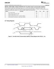
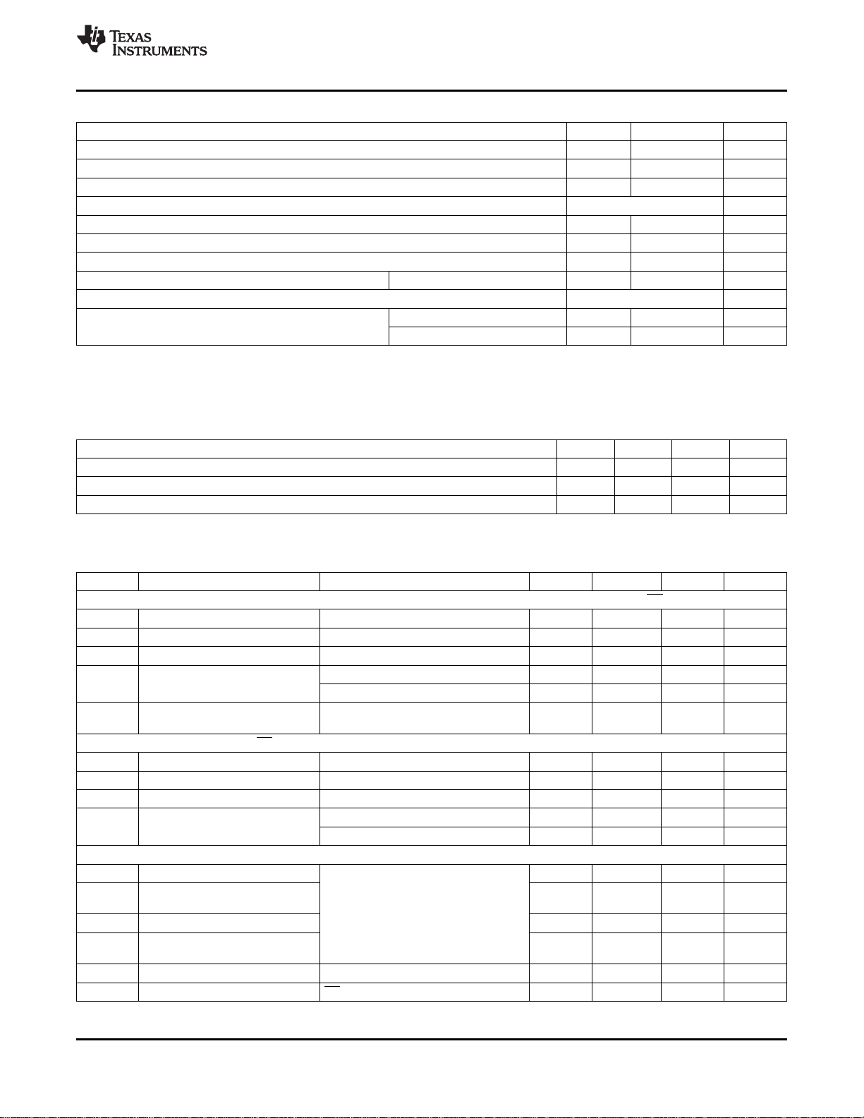
Electrical Characteristics
Over recommended operating supply and temperature ranges unless otherwise specified.
(1)
Symbol Parameter Conditions Min Typ Max Unit
LVCMOS/LVTTL DC SPECIFICATIONS ( All pins, except output pins AnP, AnM, CLKnP and CLKnM, BAL, PD pins)
V
IH
High Level Input Voltage V
REF
= V
CC3V
= V
CC
2.0 V
CC
V
V
IL
Low Level Input Voltage V
REF
= V
CC3V
= V
CC
GND 0.8 V
V
CL
Input Clamp Voltage I
CL
= 18 mA -0.8 -1.5 V
I
IN
Input Current V
IN
= 0.4V, or V
CC
+1.8 +15 µA
V
IN
= GND −15 0 µA
V
OL
Low level Open Drain Output I
OL
= 2 mA 0.1 0.3 V
Voltage
LVCMOS DC SPECIFICATIONS ( PD pin)
V
IH
High Level Input Voltage V
REF
= V
CC3V
= V
CC
2.9 V
CC
V
V
IL
Low Level Input Voltage V
REF
= V
CC3V
= V
CC
GND 0.8 V
V
CL
Input Clamp Voltage I
CL
= 18 mA -0.8 -1.5 V
I
IN
Input Current V
IN
= 0.4V, or V
CC
+1.8 +15 µA
V
IN
= GND −15 0 µA
LVDS DRIVER DC SPECIFICATIONS (output pins AnP, AnM, CLKnP and CLKnM)
V
OD
Differential Output Voltage R
L
= 100Ω 247 345 550 mV
ΔV
OD
Change in V
OD
between 35 mV
Complimentary Output States
V
OS
Offset Voltage 1.125 1.25 1.475 V
ΔV
OS
Change in V
OS
between 35 mV
Complimentary Output States
I
OS
Output Short Circuit Current V
OUT
= 0V, R
L
= 100Ω −3.5 −11 mA
I
OZ
Output TRI-STATE Current PD = 0V, V
OUT
= 0V or V
CC
±1 ±10 µA
(1) Typical values are given for V
CC
= 3.3V and T
A
= +25°C. Device tested in Non-Balanced mode only.
Copyright © 2000–2014, Texas Instruments Incorporated Submit Documentation Feedback 3
Product Folder Links: DS90C387R
器件 Datasheet 文档搜索
AiEMA 数据库涵盖高达 72,405,303 个元件的数据手册,每天更新 5,000 多个 PDF 文件
