Datasheet 搜索 > DSP数字信号处理器 > Freescale(飞思卡尔) > DSP56303VL100 数据手册 > DSP56303VL100 数据手册 3/109 页
 器件3D模型
¥ 245.605
DSP56303VL100 数据手册 - Freescale(飞思卡尔)
制造商:
Freescale(飞思卡尔)
分类:
DSP数字信号处理器
封装:
BGA-196
Pictures:
3D模型
符号图
焊盘图
引脚图
产品图
页面导航:
原理图在P1
型号编码规则在P108
封装信息在P3P67P68P70P72P74P76P78P80P82P84
技术参数、封装参数在P1P3P4P5P6P7P8P9P10P11P12P13
应用领域在P4
电气规格在P22P23P25P27P29P31P33P35P37P39P41P43
导航目录
DSP56303VL100数据手册
Page:
of 109 Go
若手册格式错乱,请下载阅览PDF原文件

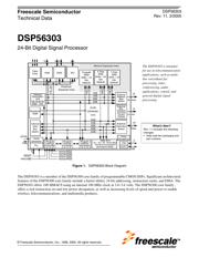
DSP56303 Technical Data, Rev. 11
Freescale Semiconductor
iii
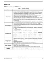
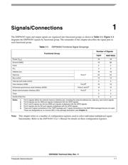
Features
Table 1 lists the features of the DSP56303 device.
Table 1. DSP56303 Features
Feature Description
High-Performance
DSP56300 Core
• 100 million multiply-accumulates per second (MMACS) with a 100 MHz clock at 3.3 V nominal
• Object code compatible with the DSP56000 core with highly parallel instruction set
• Data arithmetic logic unit (Data ALU) with fully pipelined 24 × 24-bit parallel multiplier-accumulator (MAC),
56-bit parallel barrel shifter (fast shift and normalization; bit stream generation and parsing), conditional
ALU instructions, and 24-bit or 16-bit arithmetic support under software control
• Program control unit (PCU) with position-independent code (PIC) support, addressing modes optimized for
DSP applications (including immediate offsets), internal instruction cache controller, internal memory-
expandable hardware stack, nested hardware DO loops, and fast auto-return interrupts
• Direct memory access (DMA) with six DMA channels supporting internal and external accesses; one-, two-
, and three-dimensional transfers (including circular buffering); end-of-block-transfer interrupts; and
triggering from interrupt lines and all peripherals
• Phase-lock loop (PLL) allows change of low-power divide factor (DF) without loss of lock and output clock
with skew elimination
• Hardware debugging support including on-chip emulation (OnCE‘) module, Joint Test Action Group (JTAG)
test access port (TAP)
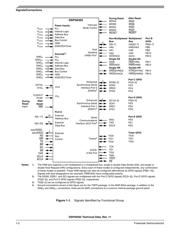
Internal Peripherals
• Enhanced 8-bit parallel host interface (HI08) supports a variety of buses (for example, ISA) and provides
glueless connection to a number of industry-standard microcomputers, microprocessors, and DSPs
• Two enhanced synchronous serial interfaces (ESSI), each with one receiver and three transmitters (allows
six-channel home theater)
• Serial communications interface (SCI) with baud rate generator
• Triple timer module
• Up to thirty-four programmable general-purpose input/output (GPIO) pins, depending on which peripherals
are enabled
Internal Memories
•192 × 24-bit bootstrap ROM
•8 K × 24-bit RAM total
• Program RAM, instruction cache, X data RAM, and Y data RAM sizes are programmable:
External Memory
Expansion
• Data memory expansion to two 256 K × 24-bit word memory spaces using the standard external address
lines
• Program memory expansion to one 256 K × 24-bit words memory space using the standard external
address lines
• External memory expansion port
• Chip select logic for glueless interface to static random access memory (SRAMs)
• Internal DRAM Controller for glueless interface to dynamic random access memory (DRAMs)
Power Dissipation
• Very low-power CMOS design
• Wait and Stop low-power standby modes
• Fully static design specified to operate down to 0 Hz (dc)
• Optimized power management circuitry (instruction-dependent, peripheral-dependent, and mode-
dependent)
Packaging
• 144-pin TQFP package in lead-free or lead-bearing versions
• 196-pin molded array plastic-ball grid array (MAP-BGA) package in lead-free or lead-bearing versions
Program RAM
Size
Instruction
Cache Size
X Data RAM
Size
Y Data RAM
Size
Instruction
Cache
Switch Mode
4096 × 24-bit 0 2048 × 24-bit 2048 × 24-bit disabled disabled
3072 × 24-bit 1024 × 24-bit 2048 × 24-bit 2048 × 24-bit enabled disabled
2048 × 24-bit 0 3072 × 24-bit 3072 × 24-bit disabled enabled
1024 × 24-bit 1024 × 24-bit 3072 × 24-bit 3072 × 24-bit enabled enabled
器件 Datasheet 文档搜索
AiEMA 数据库涵盖高达 72,405,303 个元件的数据手册,每天更新 5,000 多个 PDF 文件
