Datasheet 搜索 > 微控制器 > Microchip(微芯) > DSPIC30F2010-20E/SOG 数据手册 > DSPIC30F2010-20E/SOG 数据手册 95/202 页

 器件3D模型
¥ 34.963
DSPIC30F2010-20E/SOG 数据手册 - Microchip(微芯)
制造商:
Microchip(微芯)
分类:
微控制器
封装:
SOIC
Pictures:
3D模型
符号图
焊盘图
引脚图
产品图
页面导航:
引脚图在P5P95P192Hot
原理图在P8P15P53P58P62P63P67P71P75P82P92P96
标记信息在P185
封装信息在P148P185P190P192P201
功能描述在P91P95
技术参数、封装参数在P117P149P153P154P156P158P180P181P192
电气规格在P57P61P113P117P155P192
导航目录
DSPIC30F2010-20E/SOG数据手册
Page:
of 202 Go
若手册格式错乱,请下载阅览PDF原文件
© 2011 Microchip Technology Inc. DS70118J-page 95
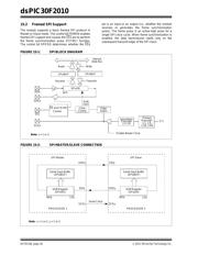
dsPIC30F2010
16.0 I
2
C™ MODULE
The Inter-Integrated Circuit (I
2
C™) module provides
complete hardware support for both Slave and Multi-
Master modes of the I
2
C serial communication
standard, with a 16-bit interface.
This module offers the following key features:
•I
2
C interface supporting both Master and Slave
operation
•I
2
C Slave mode supports 7-bit and 10-bit
addressing
•I
2
C Master mode supports 7-bit and 10-bit
addressing
•I
2
C port allows bidirectional transfers between
master and slaves
• Serial clock synchronization for I
2
C port can be
used as a handshake mechanism to suspend and
resume serial transfer (SCLREL control)
•I
2
C supports Multi-Master operation; detects bus
collision and will arbitrate accordingly
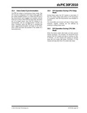
16.1 Operating Function Description
The hardware fully implements all the master and slave
functions of the I
2
C Standard and Fast mode
specifications, as well as 7- and 10-bit addressing.
Thus, the I
2
C module can operate either as a slave or
a master on an I
2
C bus.
16.1.1 VARIOUS I
2
C MODES
The following types of I
2
C operation are supported:
•I
2
C Slave operation with 7-bit addressing
•I
2
C Slave operation with 10-bit addressing
•I
2
C Master operation with 7-bit or 10-bit addressing
See the I
2
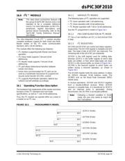
C programmer’s model in Figure 16-1.
16.1.2 PIN CONFIGURATION IN I
2
C MODE
I
2
C has a 2-pin interface: pin SCL is clock and pin SDA
is data.
16.1.3 I
2
C REGISTERS
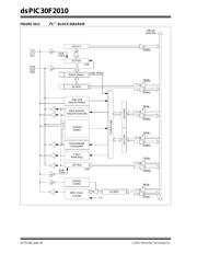
I2CCON and I2CSTAT are control and status registers,
respectively. The I2CCON register is readable and writ-
able. The lower 6 bits of I2CSTAT are read-only. The
remaining bits of the I2CSTAT are read/write.
I2CRSR is the shift register used for shifting data,
whereas I2CRCV is the buffer register to which data
bytes are written, or from which data bytes are read.
I2CRCV is the receive buffer, as shown in Figure 16-1.
I2CTRN is the transmit register to which bytes are
written during a transmit operation, as shown in
Figure 16-2.
The I2CADD register holds the slave address. A status
bit, ADD10, indicates 10-bit Address mode. The
I2CBRG acts as the Baud Rate Generator (BRG)
reload value.
In receive operations, I2CRSR and I2CRCV together
form a double-buffered receiver. When I2CRSR
receives a complete byte, it is transferred to I2CRCV
and an interrupt pulse is generated. During
transmission, the I2CTRN is not double-buffered.
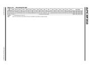
FIGURE 16-1: PROGRAMMER’S MODEL
Note: This data sheet summarizes features of
this group of dsPIC30F devices and is not
intended to be a complete reference
source. For more information on the CPU,
peripherals, register descriptions and
general device functionality, refer to the
“dsPIC30F Family Reference Manual”
(DS70046).
Note: Following a Restart condition in 10-bit
mode, the user only needs to match the
first 7-bit address.
bit 7
bit 0
I2CRCV (8 bits)
bit 7
bit 0
I2CTRN (8 bits)
bit 8
bit 0
I2CBRG (9 bits)
bit 15
bit 0
I2CCON (16 bits)
bit 15
bit 0
I2CSTAT (16 bits)
bit 9
bit 0
I2CADD (10 bits)
器件 Datasheet 文档搜索
AiEMA 数据库涵盖高达 72,405,303 个元件的数据手册,每天更新 5,000 多个 PDF 文件
