Datasheet 搜索 > FPGA芯片 > Altera(阿尔特拉) > EP1C4F400C8N 数据手册 > EP1C4F400C8N 数据手册 158/386 页
 器件3D模型
¥ 72.455
EP1C4F400C8N 数据手册 - Altera(阿尔特拉)
制造商:
Altera(阿尔特拉)
分类:
FPGA芯片
封装:
FBGA-400
描述:
可编程逻辑器件(CPLD/FPGA) EP1C4F400C8N FBGA-400
Pictures:
3D模型
符号图
焊盘图
引脚图
产品图
页面导航:
引脚图在P162P314P317P377Hot
典型应用电路图在P25P27P29P31P255P273
原理图在P22P141P341
封装尺寸在P12P117P377P383P384
型号编码规则在P11P117
功能描述在P21P148P149P150P152P336P338P340
技术参数、封装参数在P85P86P87P88P89P90P94P113P114P142P224P225
应用领域在P102P203P228
电气规格在P225
导航目录
EP1C4F400C8N数据手册
Page:
of 386 Go
若手册格式错乱,请下载阅览PDF原文件

6–36 Altera Corporation
Preliminary May 2008
Cyclone Device Handbook, Volume 1
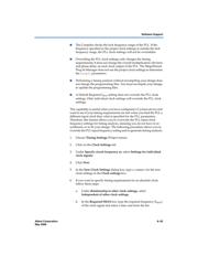
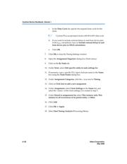
c. In the Duty Cycle list, specify the required duty cycle for the
clock.
1 Cyclone PLLs accept input clocks with 40 to 60% duty cycle.
d. If you want to include external delays to and from device pins
in the f
MAX
calculations, turn on Include external delays to and
from device pins in fMAX calculations.
e. Click OK.
7. Click OK to close the Timing Settings window.
8. Open the Assignment Organizer dialog box (Tools menu).
9. Click on the By Node tab.
10. Under Mode, select Edit specific entity & node settings for.
11. If necessary, copy a specific PLL input clock pin name to the Name
box using the Node Finder dialog box.
12. Under Assignment Categories, click the + icon next to Timing.
13. Click on Click here to add a new assignment.
14. Under Assignment, select Clock Settings in the Name list, and
select the <name> of the clock settings you created in step 5.
15. Under Stored in assignments for, select This instance only, This
instance in all occurrences of its parent entity, or Other.
16. Click Add.
17. Click OK or Apply.
18. Select Start Timing Analysis (Processing Menu).
器件 Datasheet 文档搜索
AiEMA 数据库涵盖高达 72,405,303 个元件的数据手册,每天更新 5,000 多个 PDF 文件
