Datasheet 搜索 > FPGA芯片 > Altera(阿尔特拉) > EP1C4F400C8N 数据手册 > EP1C4F400C8N 数据手册 257/386 页
 器件3D模型
¥ 72.455
EP1C4F400C8N 数据手册 - Altera(阿尔特拉)
制造商:
Altera(阿尔特拉)
分类:
FPGA芯片
封装:
FBGA-400
描述:
可编程逻辑器件(CPLD/FPGA) EP1C4F400C8N FBGA-400
Pictures:
3D模型
符号图
焊盘图
引脚图
产品图
页面导航:
引脚图在P162P314P317P377Hot
典型应用电路图在P25P27P29P31P255P273
原理图在P22P141P341
封装尺寸在P12P117P377P383P384
型号编码规则在P11P117
功能描述在P21P148P149P150P152P336P338P340
技术参数、封装参数在P85P86P87P88P89P90P94P113P114P142P224P225
应用领域在P102P203P228
电气规格在P225
导航目录
EP1C4F400C8N数据手册
Page:
of 386 Go
若手册格式错乱,请下载阅览PDF原文件
Altera Corporation 12–3
May 2008 Preliminary
Voltage Regulators
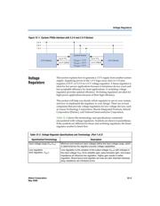
Figure 12–1. Cyclone FPGAs Interface with 3.3-V and 2.5-V Devices
Voltage
Regulators
This section explains how to generate a 1.5-V supply from another system
supply. Supplying power to the 1.5-V logic array and/or I/O pins
requires a 5.0-V- or 3.3-V-to-1.5-V voltage regulator. A linear regulator is
ideal for low-power applications because it minimizes device count and
has acceptable efficiency for most applications. A switching voltage
regulator provides optimal efficiency. Switching regulators are ideal for
high-power applications because of their high efficiency.
This section will help you decide which regulator to use in your system,
and how to implement the regulator in your design. There are several
companies that provide voltage regulators for low-voltage devices, such
as Linear Technology Corporation, Maxim Integrated Products, Intersil
Corporation (Elantec), and National Semiconductor Corporation.
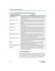
Table 12–2 shows the terminology and specifications commonly
encountered with voltage regulators. Symbols are shown in parentheses.
If the symbols are different for linear and switching regulators, the linear
regulator symbol is listed first.
3.3 V
2.5 V
1.5 V
3.3-V TTL
3.3-V CMOS
3.3-V Device 2.5-V Device
Cyclone Device
2.5-V TTL
2.5-V CMOS
V
CCINT
= 1.5 V
V
CCIO1
= 2.5 V
V
CCIO2
= 3.3 V
Table 12–2. Voltage Regulator Specifications and Terminology (Part 1 of 2)
Specification/Terminology Description
Input voltage range (V
IN
,V
CC
) Minimum and maximum input voltages define the input voltage range, which
is determined by the regulator process voltage capabilities.
Line regulation
(line regulation, V
OUT
)
Line regulation is the variation of the output voltage (V
OUT
) with changes in
the input voltage (V
IN
). Error amplifier gain, pass transistor gain, and output
impedance all influence line regulation. Higher gain results in better
regulation. Board layout and regulator pin-outs are also important because
stray resistance can introduce errors.
器件 Datasheet 文档搜索
AiEMA 数据库涵盖高达 72,405,303 个元件的数据手册,每天更新 5,000 多个 PDF 文件
