Datasheet 搜索 > FPGA芯片 > Altera(阿尔特拉) > EP2S15F484C3 数据手册 > EP2S15F484C3 数据手册 3/248 页
 器件3D模型
¥ 2644.089
EP2S15F484C3 数据手册 - Altera(阿尔特拉)
制造商:
Altera(阿尔特拉)
分类:
FPGA芯片
封装:
FBGA-484
描述:
FPGA - 现场可编程门阵列 FPGA - Stratix II 780 LABs 342 IOs
Pictures:
3D模型
符号图
焊盘图
引脚图
产品图
页面导航:
原理图在P20P25P61P144
封装尺寸在P247
型号编码规则在P7P247
功能描述在P19P20
技术参数、封装参数在P141P142P147P150P151P152P154P155P156P157P158P159
应用领域在P174P175P176P177P178P179
电气规格在P136P149
型号编号列表在P147
导航目录
EP2S15F484C3数据手册
Page:
of 248 Go
若手册格式错乱,请下载阅览PDF原文件

Altera Corporation iii
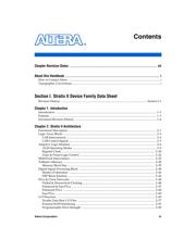
Contents
Chapter Revision Dates .......................................................................... vii
About this Handbook ................................................................................ i
How to Contact Altera ............................................................................................................................... i
Typographic Conventions ......................................................................................................................... i
Section I. Stratix II Device Family Data Sheet
Revision History ....................................................................................................................... Section I–1
Chapter 1. Introduction
Introduction ............................................................................................................................................ 1–1
Features ................................................................................................................................................... 1–1
Document Revision History ................................................................................................................. 1–6
Chapter 2. Stratix II Architecture
Functional Description .......................................................................................................................... 2–1
Logic Array Blocks ................................................................................................................................ 2–3
LAB Interconnects ............................................................................................................................ 2–4
LAB Control Signals ......................................................................................................................... 2–5
Adaptive Logic Modules ...................................................................................................................... 2–6
ALM Operating Modes ................................................................................................................... 2–9
Register Chain ................................................................................................................................. 2–20
Clear & Preset Logic Control ........................................................................................................ 2–22
MultiTrack Interconnect ..................................................................................................................... 2–22
TriMatrix Memory ............................................................................................................................... 2–28
Memory Block Size ......................................................................................................................... 2–29
Digital Signal Processing Block ......................................................................................................... 2–40
Modes of Operation ....................................................................................................................... 2–44
DSP Block Interface ........................................................................................................................ 2–44
PLLs & Clock Networks ..................................................................................................................... 2–48
Global & Hierarchical Clocking ................................................................................................... 2–48
Enhanced & Fast PLLs ................................................................................................................... 2–57
Enhanced PLLs ............................................................................................................................... 2–68
Fast PLLs .......................................................................................................................................... 2–69
I/O Structure ........................................................................................................................................ 2–69
Double Data Rate I/O Pins ........................................................................................................... 2–77
External RAM Interfacing ............................................................................................................. 2–81
Programmable Drive Strength .....................................................................................................2–83
器件 Datasheet 文档搜索
AiEMA 数据库涵盖高达 72,405,303 个元件的数据手册,每天更新 5,000 多个 PDF 文件
