Datasheet 搜索 > Intel(英特尔) > EP4CE6E22I8LN 数据手册 > EP4CE6E22I8LN 数据手册 18/490 页

 器件3D模型
¥ 130.242
EP4CE6E22I8LN 数据手册 - Intel(英特尔)
制造商:
Intel(英特尔)
封装:
LQFP-144
Pictures:
3D模型
符号图
焊盘图
引脚图
产品图
页面导航:
引脚图在P72P149P213P249P265P281Hot
典型应用电路图在P9P17P18P22P29P30P31P32P33P34P233
原理图在P41P82P83P234P250P254P285P286P290P293P295P297
型号编码规则在P26
封装信息在P26P153
功能描述在P233
技术参数、封装参数在P63P103P153P265P266P448P454P457P458P459P460P461
应用领域在P93P249
电气规格在P447

导航目录
EP4CE6E22I8LN数据手册
Page:
of 490 Go
若手册格式错乱,请下载阅览PDF原文件
1–4 Chapter 1: Cyclone IV FPGA Device Family Overview
Device Resources
Cyclone IV Device Handbook, March 2016 Altera Corporation
Volume 1
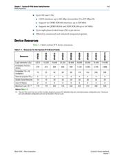
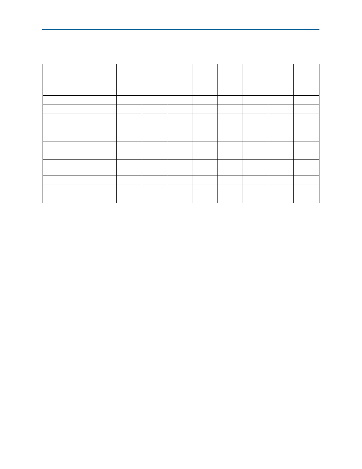
Tab le 1 –2 lists Cyclone IV GX device resources.
Table 1–2. Resources for the Cyclone IV GX Device Family
Resources
EP4CGX15
EP4CGX22
EP4CGX30
(1)
EP4CGX30
(2)
EP4CGX50
(3)
EP4CGX75
(3)
EP4CGX110
(3)
EP4CGX150
(3)
Logic elements (LEs) 14,400 21,280 29,440 29,440 49,888 73,920 109,424 149,760
Embedded memory (Kbits) 540 756 1,080 1,080 2,502 4,158 5,490 6,480
Embedded 18 × 18 multipliers 0 40 80 80 140 198 280 360
General purpose PLLs 1 2 2 4
(4)
4
(4)
4
(4)
4
(4)
4
(4)
Multipurpose PLLs 2
(5)
2
(5)
2
(5)
2
(5)
4
(5)
4
(5)
4
(5)
4
(5)
Global clock networks 20 20 20 30 30 30 30 30
High-speed transceivers
(6)
24448888
Transceiver maximum data rate
(Gbps)
2.5 2.5 2.5 3.125 3.125 3.125 3.125 3.125
PCIe (PIPE) hard IP blocks 11111111
User I/O banks 9
(7)
9
(7)
9
(7)
11
(8)
11
(8)
11
(8)
11
(8)
11
(8)
Maximum user I/O
(9)
72 150 150 290 310 310 475 475
Notes to Table 1–2:
(1) Applicable for the F169 and F324 packages.
(2) Applicable for the F484 package.
(3) Only two multipurpose PLLs for F484 package.
(4) Two of the general purpose PLLs are able to support transceiver clocking. For more information, refer to the Clock Networks and PLLs in
Cyclone IV Devices chapter.
(5) You can use the multipurpose PLLs for general purpose clocking when they are not used to clock the transceivers. For more information, refer
to the Clock Networks and PLLs in Cyclone IV Devices chapter.
(6) If PCIe 1, you can use the remaining transceivers in a quad for other protocols at the same or different data rates.
(7) Including one configuration I/O bank and two dedicated clock input I/O banks for HSSI reference clock input.
(8) Including one configuration I/O bank and four dedicated clock input I/O banks for HSSI reference clock input.
(9) The user I/Os count from pin-out files includes all general purpose I/O, dedicated clock pins, and dual purpose configuration pins. Transceiver
pins and dedicated configuration pins are not included in the pin count.
器件 Datasheet 文档搜索
AiEMA 数据库涵盖高达 72,405,303 个元件的数据手册,每天更新 5,000 多个 PDF 文件
