Datasheet 搜索 > FPGA芯片 > Altera(阿尔特拉) > EP4CGX75DF27C7N 数据手册 > EP4CGX75DF27C7N 数据手册 5/44 页
 器件3D模型
¥ 1883.063
EP4CGX75DF27C7N 数据手册 - Altera(阿尔特拉)
制造商:
Altera(阿尔特拉)
分类:
FPGA芯片
封装:
FBGA-672
Pictures:
3D模型
符号图
焊盘图
引脚图
产品图
页面导航:
技术参数、封装参数在P2P8P11P12P13P14P15P17P23P24P25P26
电气规格在P1

导航目录
EP4CGX75DF27C7N数据手册
Page:
of 44 Go
若手册格式错乱,请下载阅览PDF原文件
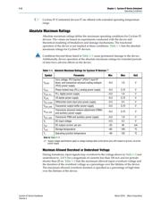
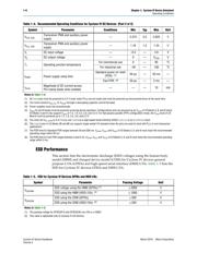
Chapter 1: Cyclone IV Device Datasheet 1–5
Operating Conditions
March 2016 Altera Corporation Cyclone IV Device Handbook,
Volume 3
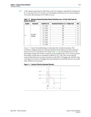
I
Diode
Magnitude of DC current across
PCI-clamp diode when enable
———10mA
Notes to Table 1–3:
(1) Cyclone IV E 1.0 V core voltage devices only support C8L, C9L, and I8L speed grades. Cyclone IV E 1.2 V core voltage devices only support
C6, C7, C8, I7, and A7 speed grades.
(2) V
CCIO
for all I/O banks must be powered up during device operation. All
VCCA
pins must be powered to 2.5 V (even when PLLs are not used)
and must be powered up and powered down at the same time.
(3) V
CC
must rise monotonically.
(4) V
CCIO
powers all input buffers.
(5) The POR time for Standard POR ranges between 50 and 200 ms. Each individual power supply must reach the recommended operating range
within 50 ms.
(6) The POR time for Fast POR ranges between 3 and 9 ms. Each individual power supply must reach the recommended operating range within
3ms.
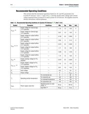
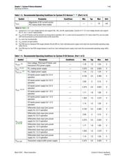
Table 1–3. Recommended Operating Conditions for Cyclone IV E Devices
(1),
(2)
(Part 2 of 2)
Symbol Parameter Conditions Min Typ Max Unit
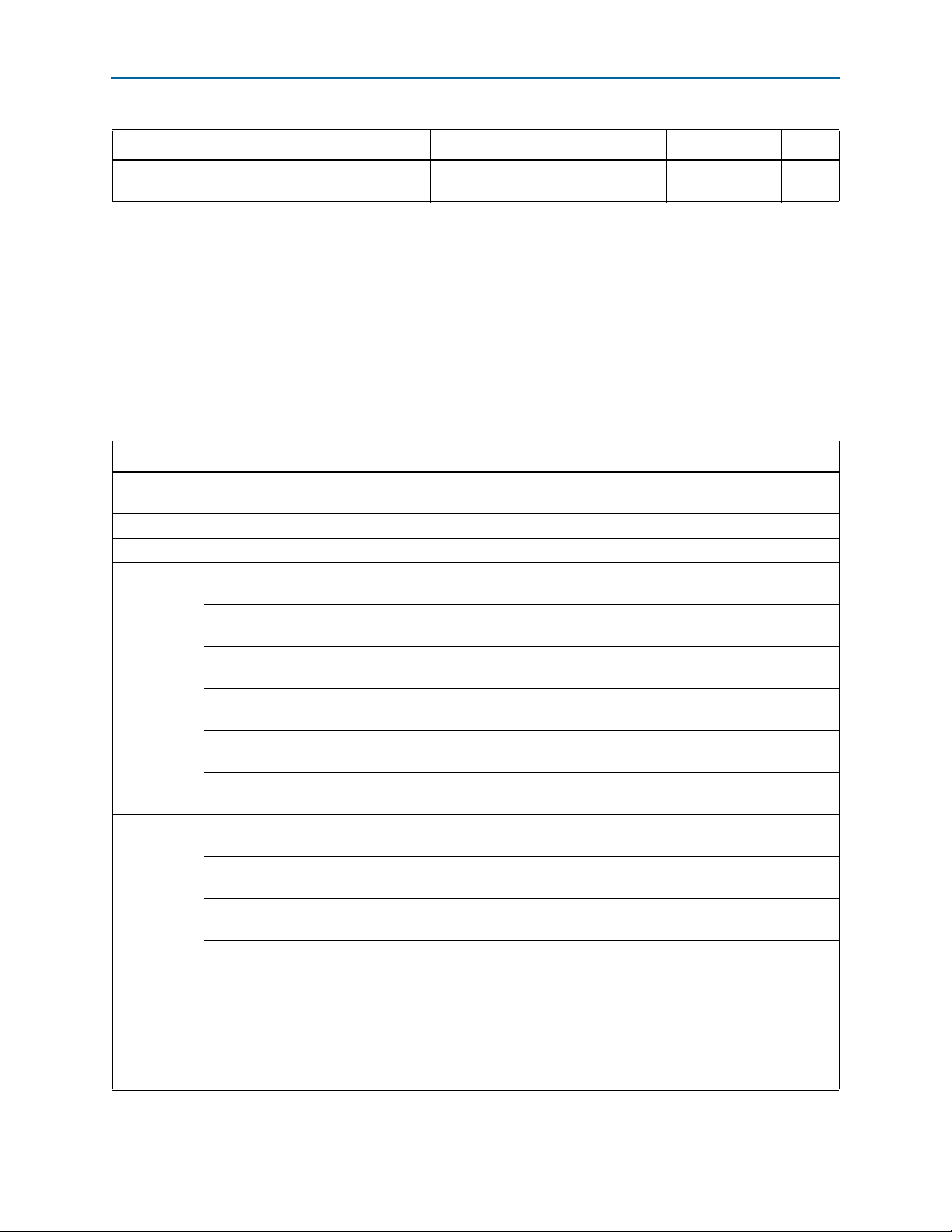
Table 1–4. Recommended Operating Conditions for Cyclone IV GX Devices (Part 1 of 2)
Symbol Parameter Conditions Min Typ Max Unit
V
CCINT
(3)
Core voltage, PCIe hard IP block, and
transceiver PCS power supply
— 1.16 1.2 1.24 V
V
CCA
(1), (3)
PLL analog power supply — 2.375 2.5 2.625 V
V
CCD_PLL
(2)
PLL digital power supply — 1.16 1.2 1.24 V
V
CCIO
(3), (4)
I/O banks power supply for 3.3-V
operation
— 3.135 3.3 3.465 V
I/O banks power supply for 3.0
-V
operation
— 2.85 3 3.15 V
I/O banks power supply for 2.5
-V
operation
— 2.375 2.5 2.625 V
I/O banks power supply for 1.8
-V
operation
— 1.71 1.8 1.89 V
I/O banks power supply for 1.5
-V
operation
— 1.425 1.5 1.575 V
I/O banks power supply for 1.2
-V
operation
— 1.14 1.2 1.26 V
V
CC_CLKIN
(3), (5), (6)
Differential clock input pins power
supply for 3.3-V operation
— 3.135 3.3 3.465 V
Differential clock input pins power
supply for 3.0
-V operation
— 2.85 3 3.15 V
Differential clock input pins power
supply for 2.5
-V operation
— 2.375 2.5 2.625 V
Differential clock input pins power
supply for 1.8
-V operation
— 1.71 1.8 1.89 V
Differential clock input pins power
supply for 1.5
-V operation
— 1.425 1.5 1.575 V
Differential clock input pins power
supply for 1.2
-V operation
— 1.14 1.2 1.26 V
V
CCH_GXB
Transceiver output buffer power supply — 2.375 2.5 2.625 V
器件 Datasheet 文档搜索
AiEMA 数据库涵盖高达 72,405,303 个元件的数据手册,每天更新 5,000 多个 PDF 文件
