Datasheet 搜索 > FPGA芯片 > Altera(阿尔特拉) > EP4CGX75DF27C7N 数据手册 > EP4CGX75DF27C7N 数据手册 6/44 页
 器件3D模型
¥ 1883.063
EP4CGX75DF27C7N 数据手册 - Altera(阿尔特拉)
制造商:
Altera(阿尔特拉)
分类:
FPGA芯片
封装:
FBGA-672
Pictures:
3D模型
符号图
焊盘图
引脚图
产品图
页面导航:
技术参数、封装参数在P2P8P11P12P13P14P15P17P23P24P25P26
电气规格在P1

导航目录
EP4CGX75DF27C7N数据手册
Page:
of 44 Go
若手册格式错乱,请下载阅览PDF原文件
1–6 Chapter 1: Cyclone IV Device Datasheet
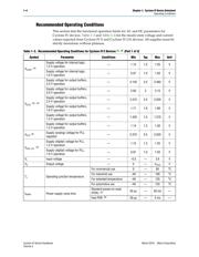
Operating Conditions
Cyclone IV Device Handbook, March 2016 Altera Corporation
Volume 3
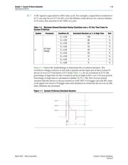
ESD Performance
This section lists the electrostatic discharge (ESD) voltages using the human body
model (HBM) and charged device model (CDM) for Cyclone IV devices general
purpose I/Os (GPIOs) and high-speed serial interface (HSSI) I/Os. Table 1–5 lists the
ESD for Cyclone IV devices GPIOs and HSSI I/Os.
V
CCA_GXB
Transceiver PMA and auxiliary power
supply
— 2.375 2.5 2.625 V
V
CCL_GXB
Transceiver PMA and auxiliary power
supply
— 1.16 1.2 1.24 V
V
I
DC input voltage — –0.5 — 3.6 V
V
O
DC output voltage — 0 — V
CCIO
V
T
J
Operating junction temperature
For commercial use 0 — 85 °C
For industrial use –40 — 100 °C
t
RAMP
Power supply ramp time
Standard power
-on reset
(POR)
(7)
50 µs — 50 ms —
Fast POR
(8)
50 µs — 3 ms —
I
Diode
Magnitude of DC current across
PCI-clamp diode when enabled
— ——10mA
Notes to Table 1–4:
(1) All
VCCA
pins must be powered to 2.5 V (even when PLLs are not used) and must be powered up and powered down at the same time.
(2) You must connect V
CCD_PLL
to V
CCINT
through a decoupling capacitor and ferrite bead.
(3) Power supplies must rise monotonically.
(4) V
CCIO
for all I/O banks must be powered up during device operation. Configurations pins are powered up by V
CCIO
of I/O Banks 3, 8, and 9 where
I/O Banks 3 and 9 only support V
CCIO
of 1.5, 1.8, 2.5, 3.0, and 3.3 V. For fast passive parallel (FPP) configuration mode, the V
CCIO
level of I/O
Bank 8 must be powered up to 1.5, 1.8, 2.5, 3.0, and 3.3 V.
(5) You must set V
CC_CLKIN
to 2.5 V if you use
CLKIN
as a high-speed serial interface (HSSI)
refclk
or as a
DIFFCLK
input.
(6) The
CLKIN
pins in I/O Banks 3B and 8B can support single-ended I/O standard when the pins are used to clock left PLLs in non-transceiver
applications.
(7) The POR time for Standard POR ranges between 50 and 200 ms. V
CCINT
, V
CCA
, and V
CCIO
of I/O Banks 3, 8, and 9 must reach the recommended
operating range within 50 ms.
(8) The POR time for Fast POR ranges between 3 and 9 ms. V
CCINT
, V
CCA
, and V
CCIO
of I/O Banks 3, 8, and 9 must reach the recommended operating
range within 3 ms.
Table 1–4. Recommended Operating Conditions for Cyclone IV GX Devices (Part 2 of 2)
Symbol Parameter Conditions Min Typ Max Unit
Table 1–5. ESD for Cyclone IV Devices GPIOs and HSSI I/Os
Symbol Parameter Passing Voltage Unit
V
ESDHBM
ESD voltage using the HBM (GPIOs)
(1)
± 2000 V
ESD using the HBM (HSSI I/Os)
(2)
± 1000 V
V
ESDCDM
ESD using the CDM (GPIOs) ± 500 V
ESD using the CDM (HSSI I/Os)
(2)
± 250 V
Notes to Table 1–5:
(1) The passing voltage for EP4CGX15 and EP4CGX30 row I/Os is ±1000V.
(2) This value is applicable only to Cyclone IV GX devices.
器件 Datasheet 文档搜索
AiEMA 数据库涵盖高达 72,405,303 个元件的数据手册,每天更新 5,000 多个 PDF 文件
