Datasheet 搜索 > Fairchild(飞兆/仙童) > F12N10L 数据手册 > F12N10L 数据手册 2/6 页


¥ 0
F12N10L 数据手册 - Fairchild(飞兆/仙童)
制造商:
Fairchild(飞兆/仙童)
Pictures:
3D模型
符号图
焊盘图
引脚图
产品图
页面导航:
型号编码规则在P1
封装信息在P1
技术参数、封装参数在P6
应用领域在P4
导航目录
F12N10L数据手册
Page:
of 6 Go
若手册格式错乱,请下载阅览PDF原文件
©2002 Fairchild Semiconductor Corporation RFP12N10L Rev. B
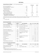
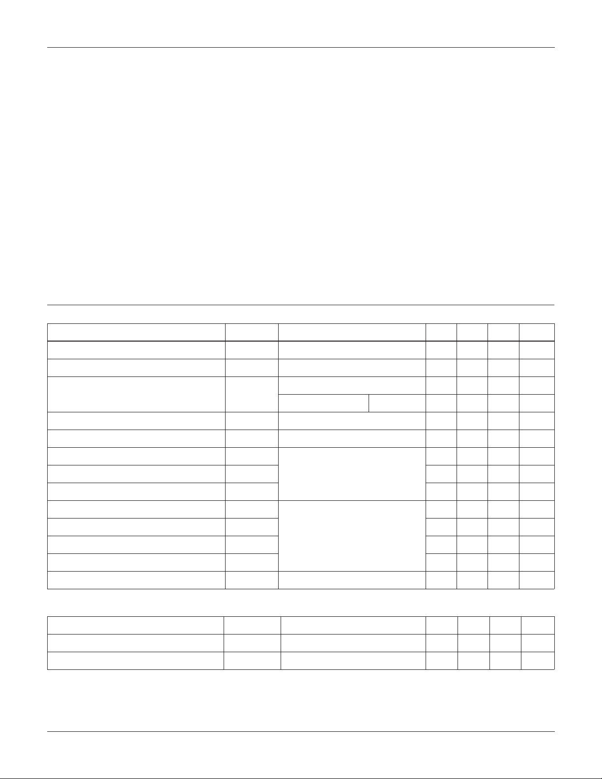
Absolute Maximum Ratings
T
C
= 25
o
C, Unless Otherwise Specified
RFP12N10L UNITS
Drain to Source Voltage (Note 1) . . . . . . . . . . . . . . . . . . . . . . . . . . . . . . . . . . . . . . . . . . . . . . . . .V
DS
100 V
Drain to Gate Voltage (R
GS
= 1M
Ω)
(Note 1) . . . . . . . . . . . . . . . . . . . . . . . . . . . . . . . . . . . . . V
DGR
100 V
Continuous Drain Current . . . . . . . . . . . . . . . . . . . . . . . . . . . . . . . . . . . . . . . . . . . . . . . . . . . . . . . I
D
12 A
Pulsed Drain Current (Note 3) . . . . . . . . . . . . . . . . . . . . . . . . . . . . . . . . . . . . . . . . . . . . . . . . . I
DM
30 A
Gate to Source Voltage . . . . . . . . . . . . . . . . . . . . . . . . . . . . . . . . . . . . . . . . . . . . . . . . . . . . . . . .V
GS
±10 V
Maximum Power Dissipation . . . . . . . . . . . . . . . . . . . . . . . . . . . . . . . . . . . . . . . . . . . . . . . . . . . . .P
D
60 W
Above T
C
= 25
o
C, Derate Linearly . . . . . . . . . . . . . . . . . . . . . . . . . . . . . . . . . . . . . . . . . . . . . . . . . 0.48 W/
o
C
Operating and Storage Temperature . . . . . . . . . . . . . . . . . . . . . . . . . . . . . . . . . . . . . . . . . . T
J,
T
STG
-55 to 150
o
C
Maximum Temperature for Soldering
Leads at 0.063in (1.6mm) from Case for 10s. . . . . . . . . . . . . . . . . . . . . . . . . . . . . . . . . . . . . . . T
L
Package Body for 10s, See Techbrief 334 . . . . . . . . . . . . . . . . . . . . . . . . . . . . . . . . . . . . . . . T
pkg
300
260
o
C
o
C
CAUTION: Stresses above those listed in “Absolute Maximum Ratings” may cause permanent damage to the device. This is a stress only rating and operation of the
device at these or any other conditions above those indicated in the operational sections of this specification is not implied.
NOTE:
1. T
J
= 25
o
C to 125
o
C.
Electrical Specifications
T
C
= 25
o
C, Unless Otherwise Specified
PARAMETER SYMBOL TEST CONDITIONS MIN TYP MAX UNITS
Drain to Source Breakdown Voltage BV
DSS
I
D
= 250mA, V
GS
= 0V 100 - - V
Gate to Threshold Voltage V
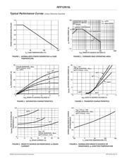
GS(TH)
V
GS
= V
DS
, I
D
= 250mA (Figure 7) 1 - 2 V
Zero Gate Voltage Drain Current I
DSS
V
DS
= 65V, V
DS
= 80V - - 1
µ
A
V
DS
= 65V, V
DS
= 80V T
C
= 125
o
C- - 50
µ
A
Gate to Source Leakage Current I
GSS
V
GS
= 10V, V
DS
= 0V - - 100
µ
A
Drain to Source On Resistance (Note 2) r
DS(ON)
I
D
= 12A, V
GS
= 5V (Figures 5, 6) - - 0.2
Ω
Input Capacitance C
ISS
V
GS
= 0V, V
DS
= 25V, f = 1MHz
(Figure 8)
- - 900 pF
Output Capacitance C
OSS
- - 325 pF
Reverse-Transfer Capacitance C
RSS
- - 170 pF
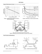
Turn-On Delay Time t
d(ON)
I
D
= 6A, V
DD
= 50V, R
G
= 6.25
Ω
,
V
GS
= 5V
(Figures 9, 10, 11)
-1550ns
Rise Time t
r
- 70 150 ns
Turn-Off Delay Time t
d(OFF)
- 100 130 ns
Fall Time t
f
- 80 150 ns
Thermal Resistance Junction to Case R
θ
JC
RFP12N10L 2.083 oC/W
Source to Drain Diode Specifications
PARAMETER SYMBOL TEST CONDITIONS MIN TYP MAX UNITS
Source to Drain Diode Voltage (Note 2) V
SD
I
SD
= 6A - - 1.4 V
Diode Reverse Recovery Time t
rr
I
SD
= 4A, dI
SD
/dt = 50A/
µ
s - 150 - ns
NOTES:
2. Pulsed: pulse duration = 80
µ
s max, duty cycle = 2%.
3. Repetitive rating: pulse width limited by maximum junction temperature.
RFP12N10L
器件 Datasheet 文档搜索
AiEMA 数据库涵盖高达 72,405,303 个元件的数据手册,每天更新 5,000 多个 PDF 文件
