Datasheet 搜索 > 电池管理芯片 > Fairchild(飞兆/仙童) > FAN54015UCX 数据手册 > FAN54015UCX 数据手册 4/36 页
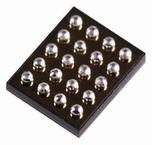
 器件3D模型
¥ 3.414
FAN54015UCX 数据手册 - Fairchild(飞兆/仙童)
制造商:
Fairchild(飞兆/仙童)
分类:
电池管理芯片
封装:
WLCSP-20
描述:
Fairchild Semiconductor### 电池管理,Fairchild Semiconductor
Pictures:
3D模型
符号图
焊盘图
引脚图
产品图
页面导航:
引脚图在P4Hot
典型应用电路图在P1
原理图在P3
封装尺寸在P35
焊盘布局在P34
型号编码规则在P2
封装信息在P2
技术参数、封装参数在P5P6P7P8P9P10
应用领域在P1
电气规格在P6P7P8
导航目录
FAN54015UCX数据手册
Page:
of 36 Go
若手册格式错乱,请下载阅览PDF原文件
© 2011 Fairchild Semiconductor Corporation www.fairchildsemi.com
FAN5401X Family • Rev. 1.0.4 4
FAN5401X Family — USB-Compliant Single-Cell Li-Ion Switching Charger with USB-OTG Boost Regulator
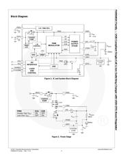
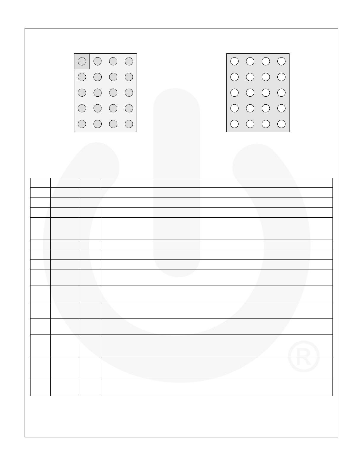
Pin Configuration
Top View
Bottom View
Figure 4. WLCSP-20 Pin Assignments
Pin Definitions
Pin # Name Part # Description
A1, A2
VBUS ALL
Charger Input Voltage and USB-OTG output voltage. Bypass with a 1
µF capacitor to PGND.
A3
NC ALL
No Connect. No external connection is made between this pin and the IC’s internal circuitry.
A4
SCL ALL
I
2
C Interface Serial Clock. This pin should not be left floating.
B1-B3
PMID ALL
Power Input Voltage. Power input to the charger regulator, bypass point for the input current
sense, and high-voltage input switch. Bypass with a minimum of 4.7
µF, 6.3 V capacitor to
PGND.
B4
SDA ALL
I
2
C Interface Serial Data. This pin should not be left floating.
C1-C3
SW ALL
Switching Node. Connect to output inductor.
C4
STAT ALL
Status. Open-drain output indicating charge status. The IC pulls this pin LOW when charging.
D1-D3
PGND ALL
Power Ground. Power return for gate drive and power transistors. The connection from this pin
to the bottom of C
MID
should be as short as possible.
D4
OTG ALL
On-The-Go. Enables boost regulator in conjunction with OTG_EN and OTG_PL bits (see Table
16). On VBUS Power-On Reset (POR), this pin sets the input current limit for t
15MIN
charging.
E1
CSIN ALL
Current-Sense Input. Connect to the sense resistor in series with the battery. The IC uses this
node to sense current into the battery. Bypass this pin with a 0.1F capacitor to PGND.
E2
AUXPWR
10, 11,
12
Auxiliary Power. Connect to the battery pack to provide IC power during High-Impedance
Mode. Bypass with a 1
µF capacitor to PGND.
E2
DISABLE
13, 14,
Charge Disable. If this pin is HIGH, charging is disabled. When LOW, charging is controlled by
the I
2
C registers. When this pin is HIGH, the 15-minute timer is reset. This pin does not affect
the 32-second timer.
E3 VREG ALL
Regulator Output. Connect to a 1 µF capacitor to PGND. This pin can supply up to 2 mA of DC
load current. For FAN54010-FAN54012, the output voltage is PMID, which is limited to 6.5 V.
For FAN54013-FAN54014, the output voltage is regulated to 1.8
V.
E4
VBAT ALL
Battery Voltage. Connect to the positive (+) terminal of the battery pack. Bypass with a 0.1
μF
capacitor to PGND if the battery is connected through long leads.
C1
B1
A1 A2
C3
B3
A3
C2
D1 D3D2
B2
C4
B4
A4
D4
E1 E3E2 E4
C1
B1
A1
C3
B3
A3 A2
C2
D1D3 D2
B2
C4
B4
A4
D4
E1E3 E2E4
器件 Datasheet 文档搜索
AiEMA 数据库涵盖高达 72,405,303 个元件的数据手册,每天更新 5,000 多个 PDF 文件
