Datasheet 搜索 > 电池管理芯片 > Fairchild(飞兆/仙童) > FAN54015UCX 数据手册 > FAN54015UCX 其他数据使用手册 1/41 页
 器件3D模型
¥ 3.408
FAN54015UCX 其他数据使用手册 - Fairchild(飞兆/仙童)
制造商:
Fairchild(飞兆/仙童)
分类:
电池管理芯片
封装:
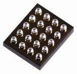
WLCSP-20
描述:
Fairchild Semiconductor### 电池管理,Fairchild Semiconductor
Pictures:
3D模型
符号图
焊盘图
引脚图
产品图
页面导航:
导航目录
FAN54015UCX数据手册
Page:
of 41 Go
若手册格式错乱,请下载阅览PDF原文件
February 2015
© 2012 Fairchild Semiconductor Corporation www.fairchildsemi.com
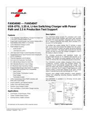
FAN54040 – FAN54047 • Rev. 1.3
FAN54040 - FAN54047— USB-OTG,1.55 A Li-Ion Switching Charger with Power Path and 2.3 A Production Test Support
FAN54040 — FAN54047
USB-OTG, 1.55 A, Li-Ion Switching Charger with Power
Path and 2.3 A Production Test Support
Features
Fully Integrated, High-Efficiency Charger for Single-Cell
Li-Ion and Li-Polymer Battery Packs
Power Path Circuit Ensures Fast System Startup with a
Dead Battery when VBUS is Connected
1.55 A Maximum Charge Current
Float Voltage Accuracy:
- 0.5% at 25°C
- 1% from 0 to 125°C
5% Input and Charge Current Regulation Accuracy
Temperature-Sense Input Prevents Auto-Charging for
JEITA Compliance
Thermal Regulation and Shutdown
4.2 V at 2.3 A Production Test Mode
5 V, 500 mA Boost Mode for USB OTG
28 V Absolute Maximum Input Voltage
6 V Maximum Input Operating Voltage
Programmable through High-Speed I
2
C Interface
(3.4 Mb/s) with Fast Mode Plus Compatibility
- Input Current
- Fast-Charge / Termination Current
- Float Voltage
- Termination Enable
3 MHz Synchronous Buck PWM Controller with
Wide Duty Cycle Range
Small Footprint 1 H External Inductor
Safety Timer with Reset Control
Dynamic Input Voltage Control
Very Low Battery Current when Charger Inactive
Applications
Cell Phones, Smart Phones, PDAs
Tablet, Portable Media Players
Gaming Device, Digital Cameras
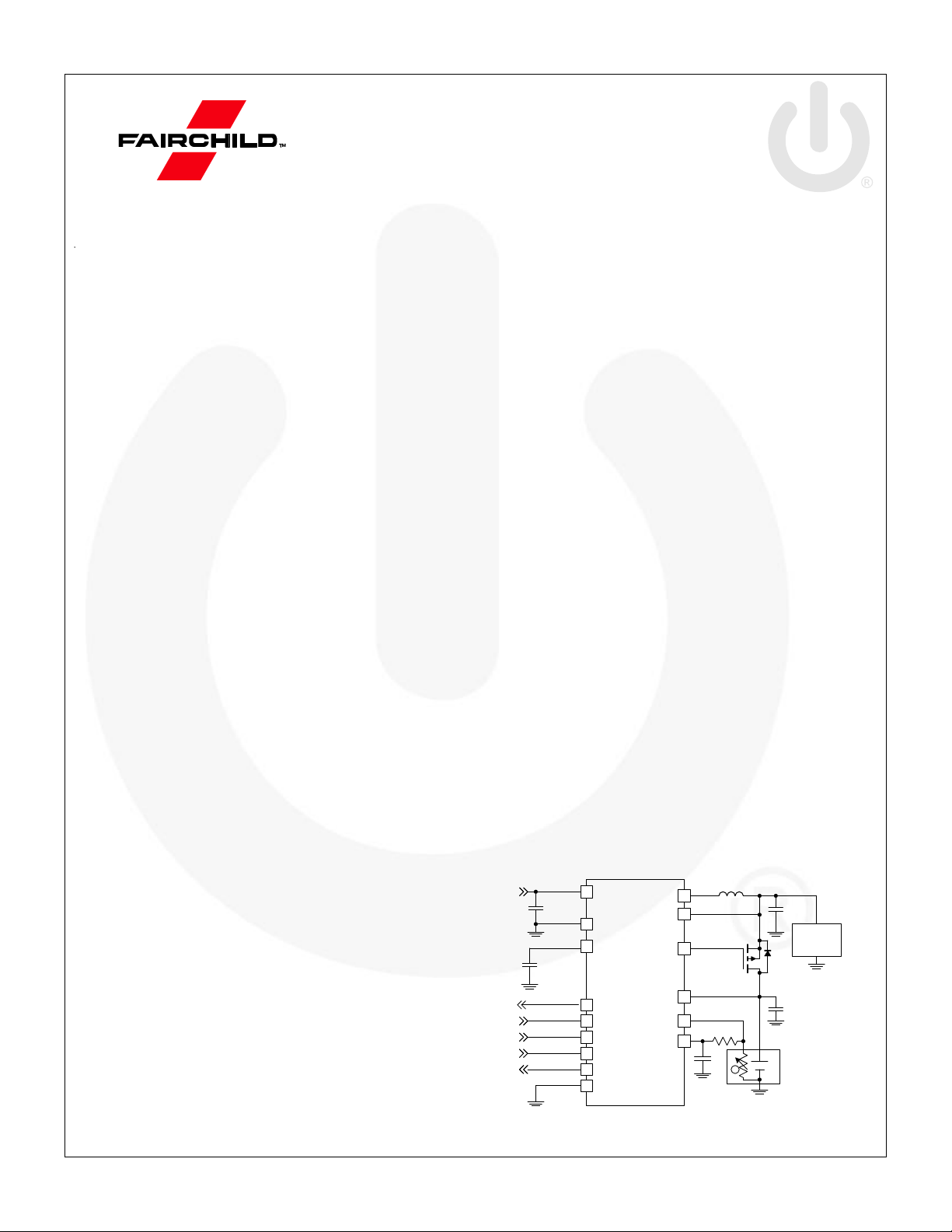
Description
The FAN5404X family includes I
2
C controlled 1.55 A USB-
compliant switch-mode chargers with power path operation
and USB OTG boost operation. Integrated with the charger,
the IC supports production test mode, which provides 4.2 V
at up to 2.3 A to the system.
To facilitate fast system startup, the IC includes a power
path circuit, which disconnects the battery from the system
rail, ensuring that the system can power up quickly following
a VBUS connection. The power path circuit ensures that the
system rail stays up when the charger is plugged in, even if
the battery is dead or shorted.
The charging parameters and operating modes are
programmable through an I
2
C Interface that operates up to
3.4 Mbps. The charger and boost regulator circuits switch at
3 MHz to minimize the size of external passive components.
The FAN5404X provides battery charging in three phases:
conditioning, constant current, and constant voltage. The
integrated circuit automatically restarts the charge cycle
when the battery falls below a voltage threshold. If the input
source is removed, the IC enters a high-impedance mode
blocking battery current from leaking to the input. Charge
status is reported back to the host through the I
2
C port.
Dynamic input voltage control prevents a weak adapter’s
voltage from collapsing, ensuring charging capability from
such adapters.
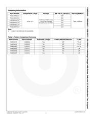
The FAN5404X is available in a 25-bump, 0.4 mm pitch,
WLCSP package.
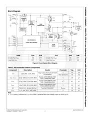
SW
SYSTEM
LOAD
L1
Q5
SDA
SCL
VBUS
C
BUS
VBAT
SYS
GATE
C
SYS
External
PMOS
POK_B
ILIM
DIS
PGND
STAT
AGND
+
PMID
C
MID
C
BAT
NTC
REF
R
REF
C
REF
T
BATTERY
FAN5404X
Figure 1. Typical Application
All trademarks are the property of their respective owners.
器件 Datasheet 文档搜索
AiEMA 数据库涵盖高达 72,405,303 个元件的数据手册,每天更新 5,000 多个 PDF 文件
