Datasheet 搜索 > TI(德州仪器) > FDC1004DSCR 数据手册 > FDC1004DSCR 数据手册 4/33 页

¥ 52.103
FDC1004DSCR 数据手册 - TI(德州仪器)
制造商:
TI(德州仪器)
封装:
WFDFN-10
描述:
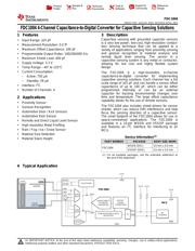
具有源屏蔽驱动器的 4 通道、16 位、电感数字转换器 10-WSON -40 to 125
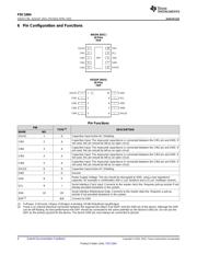
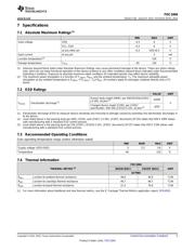
Pictures:
3D模型
符号图
焊盘图
引脚图
产品图
页面导航:
引脚图在P4Hot
典型应用电路图在P1P21P22
原理图在P10
封装尺寸在P25P27P28P30
焊盘布局在P31
标记信息在P25
封装信息在P24P25P26P27P28
技术参数、封装参数在P5P6P16
应用领域在P1P10P20P24P33
电气规格在P6P16
导航目录
FDC1004DSCR数据手册
Page:
of 33 Go
若手册格式错乱,请下载阅览PDF原文件
1
2
3
4
5
10
9
8
7
6
SHLD1
CIN1
CIN2
CIN3
CIN4
SDA
SCL
VDD
GND
SHLD2
CIN1
CIN2
CIN3
CIN4
5
4
3
2
1
6
7
8
9
10
DAP
SHLD1
SDA
SCL
VDD
GND
SHLD2
FDC1004
SNOSCY5B –AUGUST 2014–REVISED APRIL 2015
www.ti.com
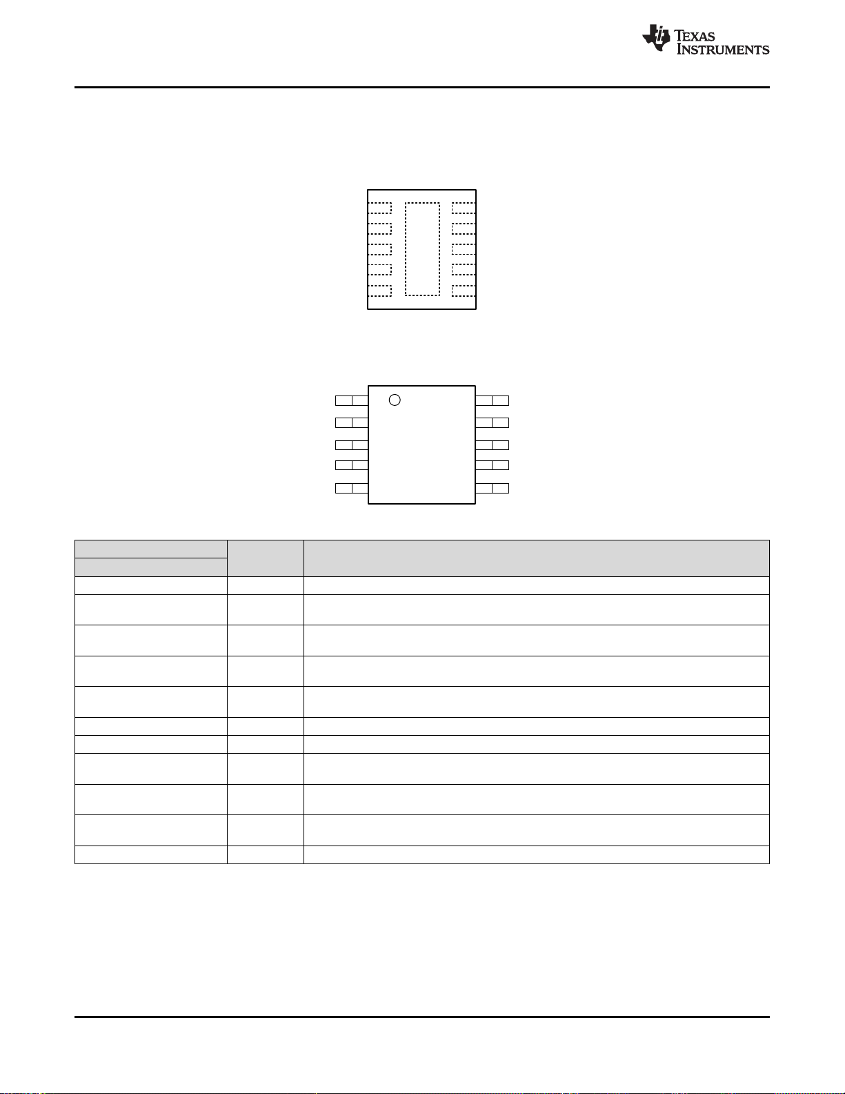
6 Pin Configuration and Functions
WSON (DSC)
10 Pins
TOP
VSSOP (DGS)
10 Pins
TOP
Pin Functions
PIN
TYPE
(1)
DESCRIPTION
NAME NO.
SHLD1 1 A Capacitive Input Active AC Shielding.
Capacitive Input. The measured capacitance is connected between the CIN1 pin and GND. If
CIN1 2 A
not used, this pin should be left as an open circuit.
Capacitive Input. The measured capacitance is connected between the CIN2 pin and GND. If
CIN2 3 A
not used, this pin should be left as an open circuit.
Capacitive Input. The measured capacitance is connected between the CIN3 pin and GND. If
CIN3 4 A
not used, this pin should be left as an open circuit.
Capacitive Input. The measured capacitance is connected between the CIN4 pin and GND. If
CIN4 5 A
not used, this pin should be left as an open circuit.
SHLD2 6 A Capacitive Input Active AC Shielding.
GND 7 G Ground
Power Supply Voltage. This pin should be decoupled to GND, using a low impedance
VDD 8 P
capacitor, for example in combination with a 1-μF tantalum and a 0.1-μF multilayer ceramic.
Serial Interface Clock Input. Connects to the master clock line. Requires pull-up resistor if not
SCL 9 I
already provided elsewhere in the system.
Serial Interface Bidirectional Data. Connects to the master data line. Requires a pull-up
SDA 10 I/O
resistor if not provided elsewhere in the system.
DAP
(2)
- N/A Connect to GND
(1) P=Power, G=Ground, I=Input, O=Output, A=Analog, I/O=Bi-Directional Input/Output
(2) There is an internal electrical connection between the exposed Die Attach Pad (DAP) and the GND pin of the device. Although the DAP
can be left floating, for best performance the DAP should be connected to the same potential as the device's GND pin. Do not use the
DAP as the primary ground for the device. The device GND pin must always be connected to ground.
4 Submit Documentation Feedback Copyright © 2014–2015, Texas Instruments Incorporated
Product Folder Links: FDC1004
器件 Datasheet 文档搜索
AiEMA 数据库涵盖高达 72,405,303 个元件的数据手册,每天更新 5,000 多个 PDF 文件
