Datasheet 搜索 > TI(德州仪器) > FDC1004DSCR 数据手册 > FDC1004DSCR 数据手册 5/33 页

¥ 52.103
FDC1004DSCR 数据手册 - TI(德州仪器)
制造商:
TI(德州仪器)
封装:
WFDFN-10
描述:
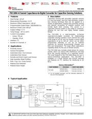
具有源屏蔽驱动器的 4 通道、16 位、电感数字转换器 10-WSON -40 to 125
Pictures:
3D模型
符号图
焊盘图
引脚图
产品图
页面导航:
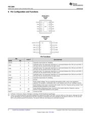
引脚图在P4Hot
典型应用电路图在P1P21P22
原理图在P10
封装尺寸在P25P27P28P30
焊盘布局在P31
标记信息在P25
封装信息在P24P25P26P27P28
技术参数、封装参数在P5P6P16
应用领域在P1P10P20P24P33
电气规格在P6P16
导航目录
FDC1004DSCR数据手册
Page:
of 33 Go
若手册格式错乱,请下载阅览PDF原文件
FDC1004
www.ti.com
SNOSCY5B –AUGUST 2014–REVISED APRIL 2015
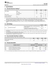
7 Specifications
7.1 Absolute Maximum Ratings
(1)
MIN MAX UNIT
Input voltage VDD –0.3 6 V
SCL, SDA –0.3 6 V
at any other pin –0.3 VDD+0.3 V
Input current at any pin 3 mA
Junction temperature
(2)
150 °C
Storage temperature T
STG
–65 150 °C
(1) Stresses beyond those listed under Absolute Maximum Ratings may cause permanent damage to the device. These are stress ratings
only, which do not imply functional operation of the device at these or any other conditions beyond those indicated under Recommended
Operating Conditions. Exposure to absolute-maximum-rated conditions for extended periods may affect device reliability.
(2) The maximum power dissipation is a function of T
J(MAX)
, R
θJA
, and the ambient temperature, T
A
. The maximum allowable power
dissipation at any ambient temperature is P
DMAX
= (T
J(MAX)
- T
A
)/ R
θJA
. All numbers apply for packages soldered directly onto a PC
board.
7.2 ESD Ratings
VALUE UNIT
Human body model (HBM), per ANSI/ESDA/JEDEC
±1000
JS-001, all pins
(2)
V
(ESD)
Electrostatic discharge
(1)
V
Charged device model (CDM), per JEDEC
±250
specification -500 500 JESD22-C101, all pins
(3)
(1) Electrostatic discharge (ESD) to measure device sensitivity and immunity to damage caused by assembly line electrostatic discharges in
to the device.
(2) Level listed above is the passing level per ANSI, ESDA, and JEDEC JS-001. JEDEC document JEP155 states that 500-V HBM allows
safe manufacturing with a standard ESD control process.
(3) Level listed above is the passing level per EIA-JEDEC JESD22-C101. JEDEC document JEP157 states that 250-V CDM allows safe
manufacturing with a standard ESD control process.
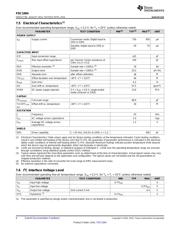
7.3 Recommended Operating Conditions
Over operating temperature range (unless otherwise noted)
MIN NOM MAX UNIT
Supply voltage (VDD-GND) 3 3.3 3.6 V
Temperature –40 125 °C
7.4 Thermal Information
FDC1004
THERMAL METRIC
(1)
WSON (DSC) VSSOP (DGS) UNIT
10 PINS
R
θJA
Junction-to-ambient thermal resistance 46.8 46.8 °C/W
R
θJC
Junction-to-case(top) thermal resistance 46.7 48.7 °C/W
R
θJB
Junction-to-board thermal resistance 21.5 70.6 °C/W
(1) For more information about traditional and new thermal metrics, see the IC Package Thermal Metrics application report, SPRA953.
Copyright © 2014–2015, Texas Instruments Incorporated Submit Documentation Feedback 5
Product Folder Links: FDC1004
器件 Datasheet 文档搜索
AiEMA 数据库涵盖高达 72,405,303 个元件的数据手册,每天更新 5,000 多个 PDF 文件
