Datasheet 搜索 > MOS管 > ON Semiconductor(安森美) > FQPF19N20 数据手册 > FQPF19N20 数据手册 1/8 页

¥ 7.191
FQPF19N20 数据手册 - ON Semiconductor(安森美)
制造商:
ON Semiconductor(安森美)
分类:
MOS管
封装:
TO-220-3
Pictures:
3D模型
符号图
焊盘图
引脚图
产品图
页面导航:
导航目录
FQPF19N20数据手册
Page:
of 8 Go
若手册格式错乱,请下载阅览PDF原文件
November 2013
FQPF19N20 — N-Channel QFET
®
MOSFET
©2000 Fairchild Semiconductor Corporation
FQPF19N20 Rev. C1
www.fairchildsemi.com
1
FQPF19N20
N-Channel QFET
®
MOSFET
200 V, 11.8 A, 150 mΩ
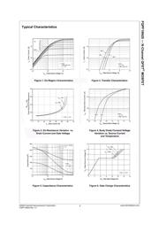
Description
This N-Channel enhancement mode power MOSFET is
produced using Fairchild Semiconductor’s proprietary
planar stripe and DMOS technology. This advanced
MOSFET technology has been especially tailored to reduce
on-state resistance, and to provide superior switching
performance and high avalanche energy strength. These
devices are suitable for switched mode power supplies,
active power factor correction (PFC), and electronic lamp
ballasts.
Features
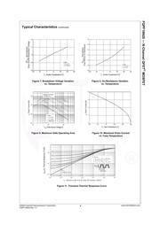
• 11.8 A, 200 V, R
DS(on)
= 150 mΩ (Max.) @ V
GS
= 10 V,
I
D
= 5.9 A
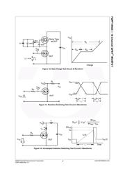
• Low Gate Charge (Typ. 31 nC)
• Low Crss (Typ. 30 pF)
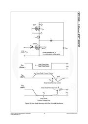
• 100% Avalanche Tested
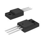
TO-220F
G
D
S
G
S
D
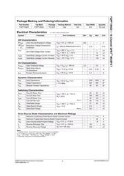
Absolute Maximum Ratings T
C
= 25°C unless otherwise noted.
Thermal Characteristics
Symbol Parameter FQPF19N20 Unit
V
DSS
Drain-Source Voltage 200 V
I
D
Drain Current
- Continuous (T
C
= 25°C)
11.8 A
- Continuous (T
C
= 100°C)
7.5 A
I
DM
Drain Current - Pulsed
(Note 1)
48 A
V
GSS
Gate-Source Voltage ± 30 V
E
AS
Single Pulsed Avalanche Energy
(Note 2)
250 mJ
I
AR
Avalanche Current
(Note 1)
11.8 A
E
AR
Repetitive Avalanche Energy
(Note 1)
5.0 mJ
dv/dt Peak Diode Recovery dv/dt
(Note 3)
5.5 V/ns
P
D
Power Dissipation (T
C
= 25°C)
50 W
- Derate above 25°C 0.4 W/°C
T
J
, T
STG
Operating and Storage Temperature Range -55 to +150 °C
T
L
Maximum Lead Temperature for Soldering,
1/8" from Case for 5 seconds
300 °C
Symbol Parameter FQPF19N20 Unit
R
θJC
Thermal Resistance, Junction-to-Case, Max. 2.5 °C/W
R
θJA
Thermal Resistance, Junction-to-Ambient, Max. 62.5 °C/W
器件 Datasheet 文档搜索
AiEMA 数据库涵盖高达 72,405,303 个元件的数据手册,每天更新 5,000 多个 PDF 文件
