Datasheet 搜索 > 模拟开关芯片 > Fairchild(飞兆/仙童) > FSA2567MPX 数据手册 > FSA2567MPX 数据手册 4/12 页
 器件3D模型
¥ 7.261
FSA2567MPX 数据手册 - Fairchild(飞兆/仙童)
制造商:
Fairchild(飞兆/仙童)
分类:
模拟开关芯片
封装:
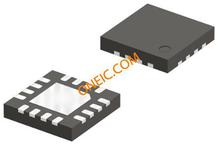
MLP
描述:
FAIRCHILD SEMICONDUCTOR FSA2567MPX 模拟开关, 4PDT, 1 放大器, 0.7 ohm, 1.65V 至 4.3V, MLP, 16 引脚 新
Pictures:
3D模型
符号图
焊盘图
引脚图
产品图
页面导航:
导航目录
FSA2567MPX数据手册
Page:
of 12 Go
若手册格式错乱,请下载阅览PDF原文件
www.onsemi.com
4
FSA2567 — Low-Power, Dual SIM Card Analog Switch
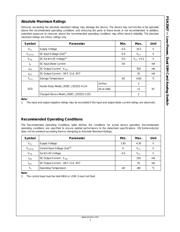
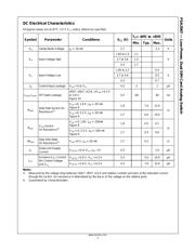
DC Electrical Characteristics
All typical values are at 25°C, 3.3 V V
CC
unless otherwise specified.
Symbol Parameter Conditions V
CC
(V)
T
A
=- 40ºC to +85ºC
Units
Min. Typ. Max.
V
IK
Clamp Diode Voltage I
IN
= -18 mA 2.7 -1.2 V
V
IH
Input Voltage High
1.65 to 2.3 1.1
V 2.7 to 3.6 1.3
4.3 1.7
V
IL
Input Voltage Low
1.65 to 2.3 0.4
V 2.7 to 3.6 0.5
4.3 0.7
I
IN
Control Input Leakage V
SW
= 0 to V
CC
4.3 -1 1 µA
I
nc(off),
I
no(off),
Off State Leakage
nRST, nDAT, nCLK, nV
SIM
= 0.3 V
or 3.6 V
Figure 10
4.3 -60 60 nA
R
OND
Data Path Switch On
Resistance
(3)
V
SW
=
0, 1.8 V, I
ON
= -20 mA
Figure 9
1.8 7.0 12.0
Ω
V
SW
=
0, 2.3 V, I
ON
= -20 mA
Figure 9
2.7 6.0 10.0
R
ONV
V
SIM
Sw itch
On Resistance
(3)
V
SW
=
0, 1.8V, I
ON
= -100mA
Figure 9
1.8 0.5 0.7
Ω
V
SW
=
0, 2.3 V, I
ON
= -100 mA
Figure 9
2.7 0.4 0.6
∆R
OND
Data Path Delta
On Resistance
(4)
V
SW
=
0 V, I
ON
=
-20 mA 2.7 0.2 Ω
I
CC
Quiescent Supply
Current
V
CNTRL
=
0 or V
CC
, I
OUT
= 0 4.3 1.0 µA
I
CCT
Increase in I
CC
Current
Per Control Voltage
and V
CC
V
CNTRL
=
2.6 V, V
CC
= 4.3 V 4.3 5.0 10.0 µA
V
CNTRL
=
1.8 V, V
CC
= 4.3 V 4.3 7.0 15.0 µA
Notes:
3. Measured by the voltage drop between nDAT, nRST, nCLK and relative common port pins at the indicated current
through the switch. On resistance is determined by the lower of the voltage on the relative ports.
4. Guaranteed by characterization.
器件 Datasheet 文档搜索
AiEMA 数据库涵盖高达 72,405,303 个元件的数据手册,每天更新 5,000 多个 PDF 文件
