Datasheet 搜索 > 时钟信号器件 > Integrated Device Technology(艾迪悌) > ICS954101DFLFT 数据手册 > ICS954101DFLFT 数据手册 3/17 页
 器件3D模型
¥ 0
ICS954101DFLFT 数据手册 - Integrated Device Technology(艾迪悌)
制造商:
Integrated Device Technology(艾迪悌)
分类:
时钟信号器件
封装:
SSOP
Pictures:
3D模型
符号图
焊盘图
引脚图
产品图
页面导航:

导航目录
ICS954101DFLFT数据手册
Page:
of 17 Go
若手册格式错乱,请下载阅览PDF原文件
3
Integrated
Circuit
Systems, Inc.
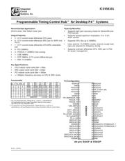
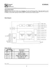
ICS954101
0815G—12/02/08
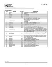
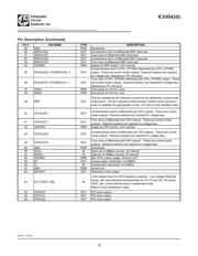
Pin Description (Continued)
Pin # PIN NAME TYPE DESCRIPTION
29 GND PWR Ground
p
in.
30 SRCCLKC5 OUT Com
p
lement clock of differential SRC clock
p
air.
31 SRCCLKT5 OUT True clock of differential SRC clock
p
air.
32 SRCCLKC6 OUT Com
p
lement clock of differential SRC clock
p
air.
33 SRCCLKT6 OUT True clock of differential SRC clock
p
air.
34 VDDSRC PWR Su
pp
l
y
for SRC clocks, 3.3V nominal
35 CPUCLKC2_ITP/SRCCLKC_7 OUT
Complimentary clock of CPU_ITP/SRC differential pair CPU_ITP/SRC
output. These are current mode outputs. External resistors are required
for volta
g
e bias. Selected b
y
ITP_EN in
p
ut.
36 CPUCLKT2_ITP/SRCCLKT_7 OUT
True clock of CPU_ITP/SRC differential pair CPU_ITP/SRC output. These
are current mode outputs. External resistors are required for voltage bias.
Selected b
y
ITP_EN in
p
ut.
37 VDDA PWR 3.3V
p
ower for the PLL core.
38 GNDA PWR Ground
p
in for the PLL core.
39 IREF OUT
This pin establishes the reference current for the differential current-mode
output pairs. This pin requires a fixed precision resistor tied to ground in
order to establish the appropriate current. 475 ohms is the standard value.
40 CPUCLKC1 OUT
Complimentary clock of differential pair CPU outputs. These are current
mode outputs. External resistors are required for voltage bias.
41 CPUCLKT1 OUT
True clock of differential pair CPU outputs. These are current mode
out
p
uts. External resistors are re
q
uired for volta
g
e bias.
42 VDDCPU PWR Su
pp
l
y
for CPU clocks, 3.3V nominal
43 CPUCLKC0 OUT
Complimentary clock of differential pair CPU outputs. These are current
mode outputs. External resistors are required for voltage bias.
44 CPUCLKT0 OUT
True clock of differential pair CPU outputs. These are current mode
out
p
uts. External resistors are re
q
uired for volta
g
e bias.
45 GND PWR Ground
p
in.
46 SCLK IN Clock
p
in of SMBus circuitr
y
, 5V tolerant.
47 SDATA I/O Data
p
in for SMBus circuitr
y
, 5V tolerant.
48 VDDREF PWR Ref, XTAL
p
ower su
pp
l
y
, nominal 3.3V
49 X2 OUT Cr
y
stal out
p
ut, Nominall
y
14.318MHz
50 X1 IN Cr
y
stal in
p
ut, Nominall
y
14.318MHz.
51 GND PWR Ground
p
in.
52 REFOUT OUT Reference Clock out
p
ut
53 FS_C/TEST_SEL IN
3.3V tolerant input for CPU frequency selection. Low voltage threshold
inputs, see input electrical characteristics for Vil_FS and Vih_FS values.
TEST_Sel: 3-level latched input to enable test mode.
Refer to Test Clarification Table
54 PCICLK0 OUT PCI clock out
p
ut.
55 PCICLK1 OUT PCI clock out
p
ut.
56 PCICLK2 OUT PCI clock output.
器件 Datasheet 文档搜索
AiEMA 数据库涵盖高达 72,405,303 个元件的数据手册,每天更新 5,000 多个 PDF 文件
