Datasheet 搜索 > 电源管理 > TI(德州仪器) > INA226AIDGST 数据手册 > INA226AIDGST 数据手册 4/38 页
 器件3D模型
¥ 6.712
INA226AIDGST 数据手册 - TI(德州仪器)
制造商:
TI(德州仪器)
分类:
电源管理
封装:
VSSOP-10
描述:
TEXAS INSTRUMENTS INA226AIDGST 电流检测放大器, 双向电流, 1个放大器, 10 µA, MSOP, 10 引脚, -40 °C, 125 °C
Pictures:
3D模型
符号图
焊盘图
引脚图
产品图
页面导航:
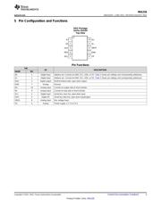
引脚图在P3Hot
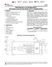
典型应用电路图在P28P29
原理图在P10P21
封装尺寸在P32P34P35
标记信息在P32
封装信息在P31P32P33P34P35
技术参数、封装参数在P4
应用领域在P1P28P29P30P38
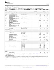
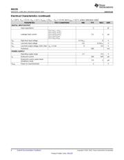
电气规格在P5P6
导航目录
INA226AIDGST数据手册
Page:
of 38 Go
若手册格式错乱,请下载阅览PDF原文件
INA226
SBOS547A –JUNE 2011–REVISED AUGUST 2015
www.ti.com
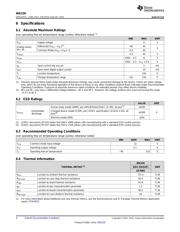
6 Specifications
6.1 Absolute Maximum Ratings
over operating free-air temperature range (unless otherwise noted)
(1)
MIN MAX UNIT
V
VS
Supply voltage 6 V
Differential (V
IN+
– V
IN-
)
(2)
–40 40
Analog Inputs,
V
IN+, IN–
Common-Mode (V
IN+
+ V
IN-
) / 2 –0.3 40
V
VBUS
–0.3 40 V
V
SDA
GND – 0.3 6 V
V
SCL
GND – 0.3 V
VS
+ 0.3 V
I
IN
Input current into any pin 5 mA
I
OUT
Open-drain digital output current 10 mA
T
J
Junction temperature 150 °C
T
stg
Storage temperature range –65 150 °C
(1) Stresses beyond those listed under Absolute Maximum Ratings may cause permanent damage to the device. These are stress ratings
only, which do not imply functional operation of the device at these or any other conditions beyond those indicated under Recommended
Operating Conditions. Exposure to absolute-maximum-rated conditions for extended periods may affect device reliability.
(2) IN+ and IN– may have a differential voltage between –40 V and 40 V. However, the voltage at these pins must not exceed the range
–0.3 V to 40 V.
6.2 ESD Ratings
VALUE UNIT
Human body model (HBM), per ANSI/ESDA/JEDEC JS-001, all pins
(1)
±2500
Electrostatic Charged device model (CDM), per JEDEC specification JESD22-C101, all
V
(ESD)
±1000 V
discharge pins
(2)
Machine model (MM) ±150
(1) JEDEC document JEP155 states that 500-V HBM allows safe manufacturing with a standard ESD control process.
(2) JEDEC document JEP157 states that 250-V CDM allows safe manufacturing with a standard ESD control process.
6.3 Recommended Operating Conditions
over operating free-air temperature range (unless otherwise noted)
MIN NOM MAX UNIT
V
CM
Common-mode input voltage 12 V
V
VS
Operating supply voltage 3.3 V
T
A
Operating free-air temperature –40 125 °C
6.4 Thermal Information
INA226
THERMAL METRIC
(1)
DGS (VSSOP) UNIT
10 PINS
R
θJA
Junction-to-ambient thermal resistance 171.4 °C/W
R
θJC(top)
Junction-to-case (top) thermal resistance 42.9 °C/W
R
θJB
Junction-to-board thermal resistance 91.8 °C/W
ψ
JT
Junction-to-top characterization parameter 1.5 °C/W
ψ
JB
Junction-to-board characterization parameter 90.2 °C/W
R
θJC(bot)
Junction-to-case (bottom) thermal resistance n/a °C/W
(1) For more information about traditional and new thermal metrics, see the Semiconductor and IC Package Thermal Metrics application
report, SPRA953.
4 Submit Documentation Feedback Copyright © 2011–2015, Texas Instruments Incorporated
Product Folder Links: INA226
器件 Datasheet 文档搜索
AiEMA 数据库涵盖高达 72,405,303 个元件的数据手册,每天更新 5,000 多个 PDF 文件
