Datasheet 搜索 > 放大器、缓冲器 > TI(德州仪器) > INA333SJD 数据手册 > INA333SJD 数据手册 2/26 页
 器件3D模型
¥ 422.983
INA333SJD 数据手册 - TI(德州仪器)
制造商:
TI(德州仪器)
分类:
放大器、缓冲器
封装:
CDIP-8
描述:
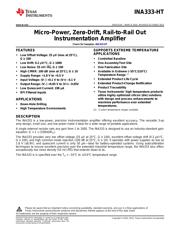
微功耗,零漂移,轨到轨输出仪表放大器 Micro-Power, Zerø-Drift, Rail-to-Rail Out Instrumentation Amplifier
Pictures:
3D模型
符号图
焊盘图
引脚图
产品图
页面导航:
导航目录
INA333SJD数据手册
Page:
of 26 Go
若手册格式错乱,请下载阅览PDF原文件
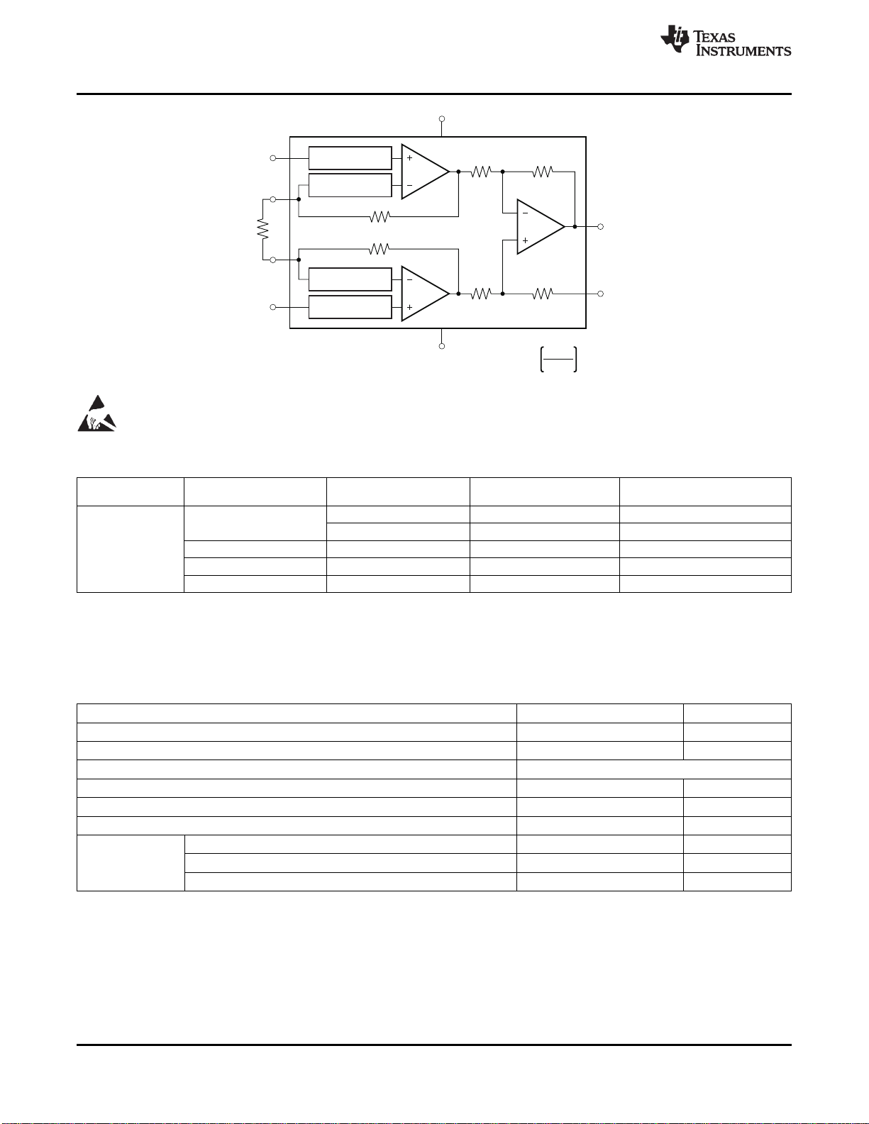
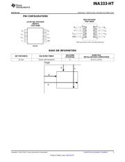
50kW
150kW 150kW
A
1
A
3
V
OUT
V
IN-
6
REF
5
RFIFilteredInputs
2
V+
7
V-
4
1
8
150kW 150kW
50kW
A
2
V
IN+
RFIFilteredInputs
3
INA333
R
G
G=1+
100kW
R
G
RFIFilteredInputs
RFIFilteredInputs
INA333-HT
SBOS514C –MARCH 2010–REVISED OCTOBER 2013
www.ti.com
This integrated circuit can be damaged by ESD. Texas Instruments recommends that all integrated circuits be handled with
appropriate precautions. Failure to observe proper handling and installation procedures can cause damage.
ESD damage can range from subtle performance degradation to complete device failure. Precision integrated circuits may be more
susceptible to damage because very small parametric changes could cause the device not to meet its published specifications.
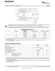
ORDERING INFORMATION
(1)
ORDERABLE PART
T
A
PACKAGE
(2)
TOP-SIDE MARKING PACKAGE QTY | CARRIER
NUMBER
INA333SKGD1 NA 240 | TRAY
KGD
INA333SKGD2 NA 10 | TRAY
–55°C to 210°C JD INA333SJD INA333SJD 1 | TUBE
HKJ INA333SHKJ INA333SHKJ 1 | TUBE
HKQ INA333SHKQ INA333SHKQ 1 | TUBE
(1) For the most current package and ordering information see the Package Option Addendum at the end of this document, or see the TI
web site at www.ti.com.
(2) Package drawings, standard packaging quantities, thermal data, symbolization, and PCB design guidelines are available at
www.ti.com/packaging.
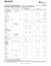
ABSOLUTE MAXIMUM RATINGS
(1)
INA333 UNIT
Supply voltage +7 V
Analog input voltage range
(2)
(V–) – 0.3 to (V+) + 0.3 V
Output short-circuit
(3)
Continuous
Operating temperature range, T
A
–55 to +210 °C
Storage temperature range, T
STG
–65 to +210 °C
Junction temperature, T
J
+210 °C
Human body model (HBM) 4000 V
ESD rating Charged device model (CDM) 1000 V
Machine model (MM) 200 V
(1) Stresses above these ratings may cause permanent damage. Exposure to absolute maximum conditions for extended periods may
degrade device reliability. These are stress ratings only, and functional operation of the device at these or any other conditions beyond
those specified is not implied.
(2) Input terminals are diode-clamped to the power-supply rails. Input signals that can swing more than 0.3V beyond the supply rails should
be current limited to 10mA or less.
(3) Short-circuit to ground.
2 Submit Documentation Feedback Copyright © 2010–2013, Texas Instruments Incorporated
Product Folder Links: INA333-HT
器件 Datasheet 文档搜索
AiEMA 数据库涵盖高达 72,405,303 个元件的数据手册,每天更新 5,000 多个 PDF 文件
