Datasheet 搜索 > CPLD芯片 > Lattice Semiconductor(莱迪思) > ISPGAL22V10AV-75LNNI 数据手册 > ISPGAL22V10AV-75LNNI 数据手册 5/19 页
 器件3D模型
¥ 0
ISPGAL22V10AV-75LNNI 数据手册 - Lattice Semiconductor(莱迪思)
制造商:
Lattice Semiconductor(莱迪思)
分类:
CPLD芯片
封装:
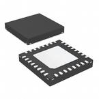
QFN-32
Pictures:
3D模型
符号图
焊盘图
引脚图
产品图
页面导航:
导航目录
ISPGAL22V10AV-75LNNI数据手册
Page:
of 19 Go
若手册格式错乱,请下载阅览PDF原文件
Lattice Semiconductor ispGAL22V10AV/B/C Data Sheet
3
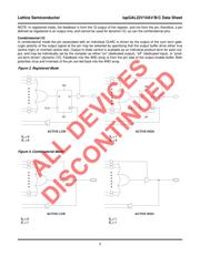
NOTE: In registered mode, the feedback is from the /Q output of the register, and not from the pin; therefore, a pin
defined as registered is an output only, and cannot be used for dynamic I/O, as can the combinatorial pins.
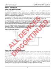
Combinatorial I/O
In combinatorial mode the pin associated with an individual OLMC is driven by the output of the sum term gate.
Logic polarity of the output signal at the pin may be selected by specifying that the output buffer drive either true
(active high) or inverted (active low). Output tri-state control is available as an individual product-term for each out-
put, and may be individually set by the compiler as either “on” (dedicated output), “off” (dedicated input), or “prod-
uct-term driven” (dynamic I/O). Feedback into the AND array is from the pin side of the output enable buffer. Both
polarities (true and inverted) of the pin are fed back into the AND array.
Figure 3. Registered Mode
Figure 4. Combinatorial Mode
ACTIVE HIGHACTIVE LOW
S
0
= 0
S
1
= 0
S
0
= 1
S
1
= 0
AR
SP
D
Q
Q
CLK
AR
SP
D
Q
QCLK
ACTIVE HIGHACTIVE LOW
S
0
= 1
S
1
= 1
S
0
= 0
S
1
= 1
ALL DEVICES
DISCONTINUED
器件 Datasheet 文档搜索
AiEMA 数据库涵盖高达 72,405,303 个元件的数据手册,每天更新 5,000 多个 PDF 文件
