Datasheet 搜索 > 稳压芯片 > TI(德州仪器) > LM1117MP-1.8/NOPB 数据手册 > LM1117MP-1.8/NOPB 数据手册 3/33 页

¥ 2.905
LM1117MP-1.8/NOPB 数据手册 - TI(德州仪器)
制造商:
TI(德州仪器)
分类:
稳压芯片
封装:
TO-261-4
描述:
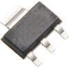
TEXAS INSTRUMENTS LM1117MP-1.8/NOPB 稳压器, 固定LDO, 15V输入, 1.2V压差, 1.8V/800mA输出, SOT-223-3
Pictures:
3D模型
符号图
焊盘图
引脚图
产品图
页面导航:
典型应用电路图在P1P10P16
原理图在P2
封装尺寸在P19P20P21P23P24P25P26
标记信息在P19P20P21P22
封装信息在P19P20P21P22P23P24P25P26
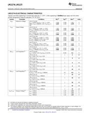
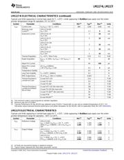
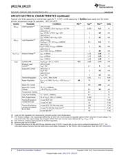
技术参数、封装参数在P3
应用领域在P1P33
电气规格在P3P4P5P6P7P8
导航目录
LM1117MP-1.8/NOPB数据手册
Page:
of 33 Go
若手册格式错乱,请下载阅览PDF原文件
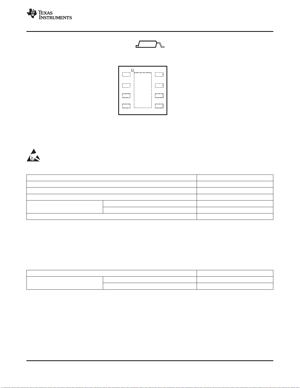
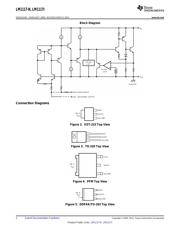
NOT CONNECTED
V
OUT
V
OUT
V
OUT
1
2
3
4
8
7
6
5
ADJ/GND
V
IN
V
IN
V
IN
V
OUT
LM1117-N, LM1117I
www.ti.com
SNOS412M –FEBRUARY 2000–REVISED MARCH 2013
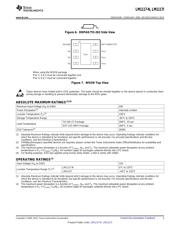
Figure 6. DDPAK/TO-263 Side View
When using the WSON package
Pins 2, 3 & 4 must be connected together and
Pins 5, 6 & 7 must be connected together
Figure 7. WSON Top View
These devices have limited built-in ESD protection. The leads should be shorted together or the device placed in conductive foam
during storage or handling to prevent electrostatic damage to the MOS gates.
ABSOLUTE MAXIMUM RATINGS
(1)(2)
Maximum Input Voltage (V
IN
to GND) 20V
Power Dissipation
(3)
Internally Limited
Junction Temperature (T
J
)
(3)
150°C
Storage Temperature Range -65°C to 150°C
TO-220 (T) Package 260°C, 10 sec
Lead Temperature
SOT-223 (IMP) Package 260°C, 4 sec
ESD Tolerance
(4)
2000V
(1) Absolute Maximum Ratings indicate limits beyond which damage to the device may occur. Operating Ratings indicate conditions for
which the device is intended to be functional, but specific performance is not ensured. For ensured specifications and the test
conditions, see the Electrical Characteristics.
(2) If Military/Aerospace specified devices are required, please contact the Texas Instruments Sales Office/Distributors for availability and
specifications.
(3) The maximum power dissipation is a function of T
J(max)
, θ
JA
, and T
A
. The maximum allowable power dissipation at any ambient
temperature is P
D
= (T
J(max)
–T
A
)/θ
JA
. All numbers apply for packages soldered directly into a PC board.
(4) For testing purposes, ESD was applied using human body model, 1.5kΩ in series with 100pF.
OPERATING RATINGS
(1)
Input Voltage (V
IN
to GND) 15V
LM1117-N 0°C to 125°C
Junction Temperature Range (T
J
)
(2)
LM1117I −40°C to 125°C
(1) Absolute Maximum Ratings indicate limits beyond which damage to the device may occur. Operating Ratings indicate conditions for
which the device is intended to be functional, but specific performance is not ensured. For ensured specifications and the test
conditions, see the Electrical Characteristics.
(2) The maximum power dissipation is a function of T
J(max)
, θ
JA
, and T
A
. The maximum allowable power dissipation at any ambient
temperature is P
D
= (T
J(max)
–T
A
)/θ
JA
. All numbers apply for packages soldered directly into a PC board.
Copyright © 2000–2013, Texas Instruments Incorporated Submit Documentation Feedback 3
Product Folder Links: LM1117-N LM1117I
器件 Datasheet 文档搜索
AiEMA 数据库涵盖高达 72,405,303 个元件的数据手册,每天更新 5,000 多个 PDF 文件
