Datasheet 搜索 > 稳压芯片 > TI(德州仪器) > LM1117MP-1.8/NOPB 数据手册 > LM1117MP-1.8/NOPB 数据手册 6/33 页

¥ 2.905
LM1117MP-1.8/NOPB 数据手册 - TI(德州仪器)
制造商:
TI(德州仪器)
分类:
稳压芯片
封装:
TO-261-4
描述:
TEXAS INSTRUMENTS LM1117MP-1.8/NOPB 稳压器, 固定LDO, 15V输入, 1.2V压差, 1.8V/800mA输出, SOT-223-3
Pictures:
3D模型
符号图
焊盘图
引脚图
产品图
页面导航:
典型应用电路图在P1P10P16
原理图在P2
封装尺寸在P19P20P21P23P24P25P26
标记信息在P19P20P21P22
封装信息在P19P20P21P22P23P24P25P26
技术参数、封装参数在P3
应用领域在P1P33
电气规格在P3P4P5P6P7P8
导航目录
LM1117MP-1.8/NOPB数据手册
Page:
of 33 Go
若手册格式错乱,请下载阅览PDF原文件
LM1117-N, LM1117I
SNOS412M –FEBRUARY 2000–REVISED MARCH 2013
www.ti.com
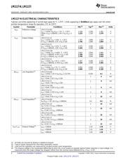
LM1117I ELECTRICAL CHARACTERISTICS (continued)
Typicals and limits appearing in normal type apply for T
J
= 25°C. Limits appearing in Boldface type apply over the entire
junction temperature range for operation, −40°C to 125°C.
Symbol Parameter Conditions Min
(1)
Typ
(2)
Max
(1)
Units
ΔV
OUT
Line Regulation
(3)
LM1117I-ADJ
I
OUT
= 10mA, 1.5V ≤ V
IN
-V
OUT
≤ 13.75V 0.035 0.3 %
LM1117I-3.3
I
OUT
= 0mA, 4.75V ≤ V
IN
≤ 15V 1 10 mV
LM1117I-5.0
I
OUT
= 0mA, 6.5V ≤ V
IN
≤ 15V 1 15 mV
ΔV
OUT
Load Regulation
(3)
LM1117I-ADJ
V
IN
-V
OUT
= 3V, 10 ≤ I
OUT
≤ 800mA 0.2 0.5 %
LM1117I-3.3
V
IN
= 4.75V, 0 ≤ I
OUT
≤ 800mA 1 15 mV
LM1117I-5.0
V
IN
= 6.5V, 0 ≤ I
OUT
≤ 800mA 1 20 mV
V
IN
-V
OUT
Dropout Voltage
(4)
I
OUT
= 100mA 1.10 1.30 V
I
OUT
= 500mA 1.15 1.35 V
I
OUT
= 800mA 1.20 1.40 V
I
LIMIT
Current Limit V
IN
-V
OUT
= 5V, T
J
= 25°C 800 1200 1500 mA
Minimum Load LM1117I-ADJ
Current
(5)
V
IN
= 15V 1.7 5 mA
Quiescent Current LM1117I-3.3
V
IN
≤ 15V 5 15 mA
LM1117I-5.0
V
IN
≤ 15V 5 15 mA
Thermal Regulation T
A
= 25°C, 30ms Pulse 0.01 0.1 %/W
Ripple Regulation f
RIPPLE
=1 20Hz, V
IN
-V
OUT
= 3V V
RIPPLE
= 60 75 dB
1V
PP
Adjust Pin Current 60 120 μA
Adjust Pin Current 10 ≤ I
OUT
≤ 800mA,
Change 1.4V ≤ V
IN
-V
OUT
≤ 10V 0.2 10 μA
Temperature Stability 0.5 %
Long Term Stability T
A
= 125°C, 1000Hrs 0.3 %
RMS Output Noise (% of V
OUT
), 10Hz ≤ f ≤10kHz 0.003 %
Thermal Resistance 3-Lead SOT-223 15.0 °C/W
Junction-to-Case
3-Lead TO-263 10 °C/W
Thermal Resistance 3-Lead SOT-223 (No heat sink) 136 °C/W
Junction-to-Ambient
3-Lead TO-263 (No heat sink)
(6)
92 °C/W
No air flow)
8-Lead WSON
(7)
40 °C/W
(3) Load and line regulation are measured at constant junction room temperature.
(4) The dropout voltage is the input/output differential at which the circuit ceases to regulate against further reduction in input voltage. It is
measured when the output voltage has dropped 100mV from the nominal value obtained at V
IN
= V
OUT
+1.5V.
(5) The minimum output current required to maintain regulation.
(6) Minimum pad size of 0.038in
2
(7) Thermal Performance for the WSON was obtained using JESD51-7 board with six vias and an ambient temperature of 22°C. For
information about improved thermal performance and power dissipation for the WSON, refer to Application Note AN-1187 (SNOA401).
6 Submit Documentation Feedback Copyright © 2000–2013, Texas Instruments Incorporated
Product Folder Links: LM1117-N LM1117I
器件 Datasheet 文档搜索
AiEMA 数据库涵盖高达 72,405,303 个元件的数据手册,每天更新 5,000 多个 PDF 文件
