Datasheet 搜索 > 运算放大器 > TI(德州仪器) > LM6172AMGWRLQV 数据手册 > LM6172AMGWRLQV 数据手册 3/25 页

¥ 4185.43
LM6172AMGWRLQV 数据手册 - TI(德州仪器)
制造商:
TI(德州仪器)
分类:
运算放大器
封装:
CFP-16
描述:
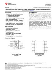
双高速,低功耗,低失真,电压反馈型放大器 Dual High Speed, Low Power, Low Distortion, Voltage Feedback Amplifiers
Pictures:
3D模型
符号图
焊盘图
引脚图
产品图
页面导航:
典型应用电路图在P18
原理图在P2P14
封装尺寸在P20P21
标记信息在P20P21P22
封装信息在P20P21P22
技术参数、封装参数在P3
应用领域在P1P22P25
电气规格在P3P4P5P6P7P8P9P10P11P12P13
导航目录
LM6172AMGWRLQV数据手册
Page:
of 25 Go
若手册格式错乱,请下载阅览PDF原文件
LM6172QML
www.ti.com
SNOSAR4A –DECEMBER 2010–REVISED OCTOBER 2011
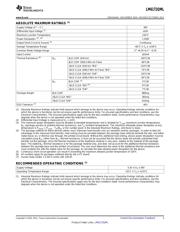
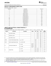
ABSOLUTE MAXIMUM RATINGS
(1)
Supply Voltage (V
+
− V
−
) 36V
Differential Input Voltage
(2)
±10V
Maximum Junction Temperature 150°C
Power Dissipation
(3)
,
(4)
1.03W
Output Short Circuit to Ground
(5)
Continuous
Storage Temperature Range −65°C ≤ T
A
≤ +150°C
Common Mode Voltage Range V
+
+0.3V to V
−
−0.3V
Input Current ±10mA
Thermal Resistance
(6)
θ
JA
8LD CDIP (Still Air) 100°C/W
8LD CDIP (500LF/Min Air Flow) 46°C/W
16LD CLGA (Still Air) “WG” 124°C/W
16LD CLGA (500LF/Min Air Flow) “WG” 74°C/W
16LD CLGA (Still Air) “GW” 135°C/W
16LD CLGA (500LF/Min Air Flow) “GW” 85°C/W
θ
JC
8LD CDIP
(4)
2°C/W
16LD CLGA “WG”
(4)
6°C/W
16LD CLGA “GW” 7°C/W
Package Weight 8LD CDIP 980mg
16LD CLGA “WG” 365mg
16LD CLGA “GW” 410mg
ESD Tolerance
(7)
4KV
(1) Absolute Maximum Ratings indicate limits beyond which damage to the device may occur. Operating Ratings indicate conditions for
which the device is functional, but do not ensure specific performance limits. For ensured specifications and test conditions, see the
Electrical Characteristics. The ensured specifications apply only for the test conditions listed. Some performance characteristics may
degrade when the device is not operated under the listed test conditions.
(2) Differential Input Voltage is measured at V
S
= ±15V.
(3) The maximum power dissipation must be derated at elevated temperatures and is dictated by T
Jmax
(maximum junction temperature),
θ
JA
(package junction to ambient thermal resistance), and T
A
(ambient temperature). The maximum allowable power dissipation at any
temperature is P
Dmax
= (T
Jmax
- T
A
)/θ
JA
or the number given in the Absolute Maximum Ratings, whichever is lower.
(4) The package material for these devices allows much improved heat transfer over our standard ceramic packages. In order to take full
advantage of this improved heat transfer, heat sinking must be provided between the package base (directly beneath the die), and either
metal traces on, or thermal vias through, the printed circuit board. Without this additional heat sinking, device power dissipation must be
calculated using θ
JA
, rather than θ
JC
, thermal resistance. It must not be assumed that the device leads will provide substantial heat
transfer out the package, since the thermal resistance of the leadframe material is very poor, relative to the material of the package
base. The stated θ
JC
thermal resistance is for the package material only, and does not account for the additional thermal resistance
between the package base and the printed circuit board. The user must determine the value of the additional thermal resistance and
must combine this with the stated value for the package, to calculate the total allowed power dissipation for the device.
(5) Continuous short circuit operation can result in exceeding the maximum allowed junction temperature of 150°C
(6) All numbers apply for packages soldered directly into a PC board.
(7) Human body model, 1.5 kΩ in series with 100 pF.
RECOMMENDED OPERATING CONDITIONS
(1)
Supply Voltage 5.5V ≤ V
S
≤ 36V
Operating Temperature Range −55°C ≤ T
A
≤ +125°C
(1) Absolute Maximum Ratings indicate limits beyond which damage to the device may occur. Operating Ratings indicate conditions for
which the device is functional, but do not ensure specific performance limits. For ensured specifications and test conditions, see the
Electrical Characteristics. The ensured specifications apply only for the test conditions listed. Some performance characteristics may
degrade when the device is not operated under the listed test conditions.
Copyright © 2010–2011, Texas Instruments Incorporated Submit Documentation Feedback 3
Product Folder Links: LM6172QML
器件 Datasheet 文档搜索
AiEMA 数据库涵盖高达 72,405,303 个元件的数据手册,每天更新 5,000 多个 PDF 文件
