Datasheet 搜索 > 运算放大器 > TI(德州仪器) > LM6172AMGWRLQV 数据手册 > LM6172AMGWRLQV 数据手册 4/25 页

¥ 4185.43
LM6172AMGWRLQV 数据手册 - TI(德州仪器)
制造商:
TI(德州仪器)
分类:
运算放大器
封装:
CFP-16
描述:
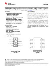
双高速,低功耗,低失真,电压反馈型放大器 Dual High Speed, Low Power, Low Distortion, Voltage Feedback Amplifiers
Pictures:
3D模型
符号图
焊盘图
引脚图
产品图
页面导航:
典型应用电路图在P18
原理图在P2P14
封装尺寸在P20P21
标记信息在P20P21P22
封装信息在P20P21P22
技术参数、封装参数在P3
应用领域在P1P22P25
电气规格在P3P4P5P6P7P8P9P10P11P12P13
导航目录
LM6172AMGWRLQV数据手册
Page:
of 25 Go
若手册格式错乱,请下载阅览PDF原文件
LM6172QML
SNOSAR4A –DECEMBER 2010–REVISED OCTOBER 2011
www.ti.com
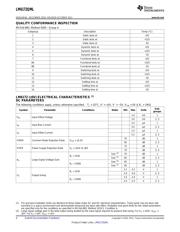
QUALITY CONFORMANCE INSPECTION
Mil-Std-883, Method 5005 - Group A
Subgroup Description Temp (°C)
1 Static tests at +25
2 Static tests at +125
3 Static tests at -55
4 Dynamic tests at +25
5 Dynamic tests at +125
6 Dynamic tests at -55
7 Functional tests at +25
8A Functional tests at +125
8B Functional tests at -55
9 Switching tests at +25
10 Switching tests at +125
11 Switching tests at -55
12 Settling time at +25
13 Settling time at +125
14 Settling time at -55
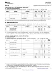
LM6172 (±5V) ELECTRICAL CHARACTERISTICS
(1)
DC PARAMETERS
The following conditions apply, unless otherwise specified. T
J
= 25°C, V
+
= +5V, V
−
= −5V, V
CM
= 0V & R
L
> 1MΩ
Sub-
Symbol Parameter Conditions Notes Min Max Units
groups
1.0 mV 1
V
IO
Input Offset Voltage
3.0 mV 2, 3
2.5 µA 1
I
IB
Input Bias Current
3.5 µA 2, 3
1.5 µA 1
I
IO
Input Offset Current
2.2 µA 2, 3
70 dB 1
CMRR Common Mode Rejection Ratio V
CM
= ±2.5V
65 dB 2, 3
75 dB 1
PSRR Power Supply Rejection Ratio V
S
= ±15V to ±5V
70 dB 2, 3
See
(2)
70 dB 1
R
L
= 1KΩ
See
(2)
65 dB 2, 3
A
V
Large Signal Voltage Gain
See
(2)
65 dB 1
R
L
= 100Ω
See
(2)
60 dB 2, 3
3.1 -3.1 V 1
R
L
= 1KΩ
3.0 -3.0 V 2, 3
V
O
Output Swing
2.5 -2.4 V 1
R
L
= 100Ω
2.4 -2.3 V 2, 3
(1) Pre and post irradiation limits are identical to those listed under AC and DC electrical characteristics. These parts may be dose rate
sensitive in a space environment and demonstrate enhanced low dose rate effect. Radiation end point limits for the noted parameters
are specified only for the conditions as specified in Mil-Std-883, Method 1019.5, Condition A.
(2) Large signal voltage gain is the total output swing divided by the input signal required to produce that swing. For V
S
= ±15V, V
OUT
=
±5V. For V
S
= ±5V, V
OUT
= ±1V.
4 Submit Documentation Feedback Copyright © 2010–2011, Texas Instruments Incorporated
Product Folder Links: LM6172QML
器件 Datasheet 文档搜索
AiEMA 数据库涵盖高达 72,405,303 个元件的数据手册,每天更新 5,000 多个 PDF 文件
