Datasheet 搜索 > DC/DC转换器 > TI(德州仪器) > LMR12007YMK 数据手册 > LMR12007YMK 数据手册 8/30 页

¥ 9.988
LMR12007YMK 数据手册 - TI(德州仪器)
制造商:
TI(德州仪器)
分类:
DC/DC转换器
封装:
TSOT-23-6
描述:
TEXAS INSTRUMENTS LMR12007YMK 直流-直流开关降压(逐步递减)稳压器, 可调, 3V-18V输入, 1.25V-16V输出, 750mA输出, SOT-6
Pictures:
3D模型
符号图
焊盘图
引脚图
产品图
页面导航:
引脚图在P2Hot
典型应用电路图在P1
原理图在P7P8
封装尺寸在P24P26P27
标记信息在P24
封装信息在P24P25P26P27
焊接温度在P2
技术参数、封装参数在P2P3
应用领域在P1
电气规格在P3P4P5P6
导航目录
LMR12007YMK数据手册
Page:
of 30 Go
若手册格式错乱,请下载阅览PDF原文件
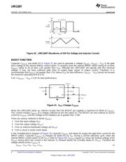
BOOST
SW
GND
L
D1
D2
C
OUT
C
BOOST
V
OUT
C
IN
V
IN
V
IN
V
BOOST
0
0
V
IN
V
D
T
ON
t
t
Inductor
Current
D = T
ON
/T
SW
V
SW
T
OFF
T
SW
I
L
I
PK
SW
Voltage
LMR12007
SNVS982 –SEPTEMBER 2013
www.ti.com
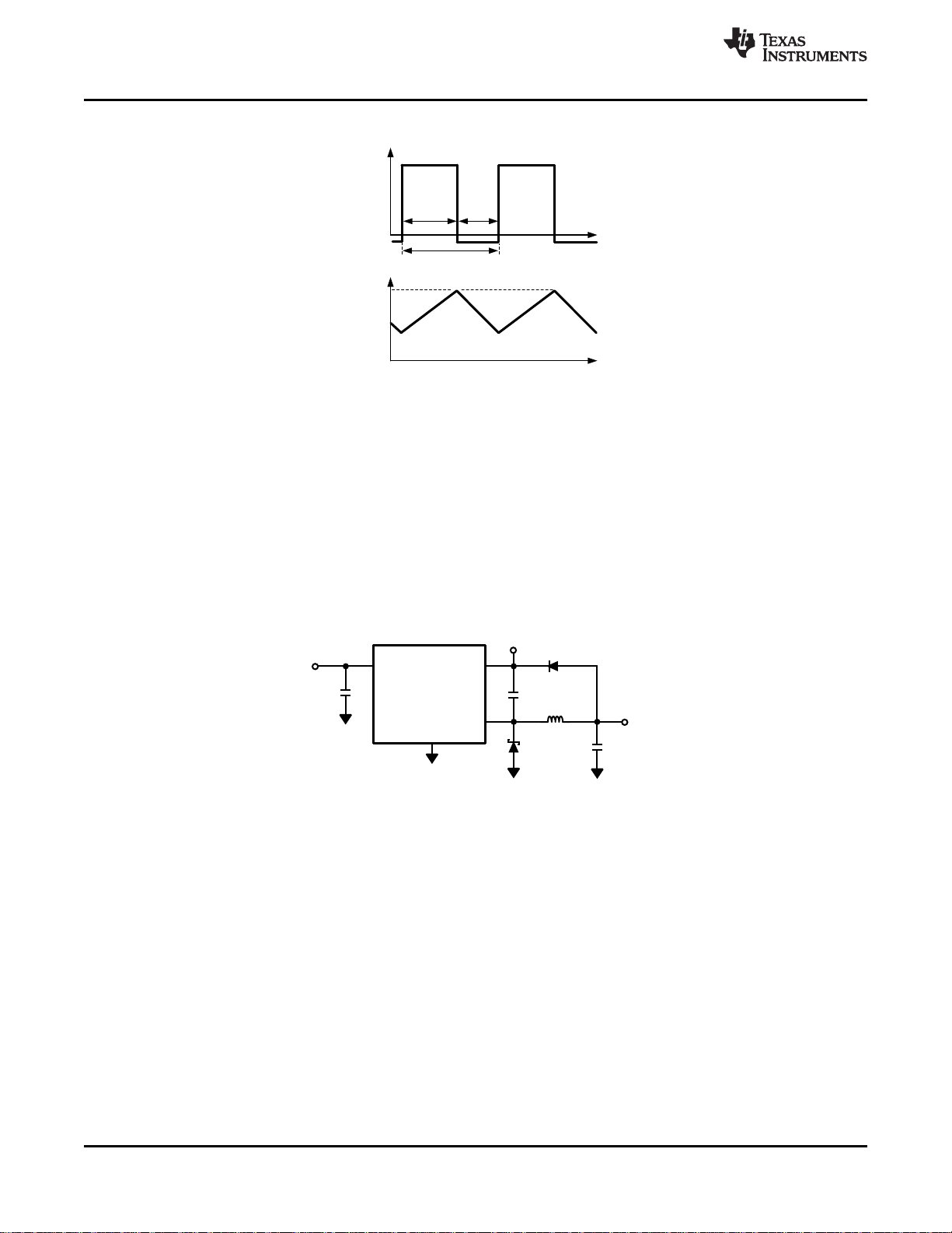
Figure 20. LMR12007 Waveforms of SW Pin Voltage and Inductor Current
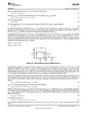
BOOST FUNCTION
Capacitor C
BOOST
and diode D2 in Figure 21 are used to generate a voltage V
BOOST
. V
BOOST
- V
SW
is the gate
drive voltage to the internal NMOS control switch. To properly drive the internal NMOS switch during its on-time,
V
BOOST
needs to be at least 1.6V greater than V
SW
. Although the LMR12007 will operate with this minimum
voltage, it may not have sufficient gate drive to supply large values of output current. Therefore, it is
recommended that V
BOOST
be greater than 2.5V above V
SW
for best efficiency. V
BOOST
– V
SW
should not exceed
the maximum operating limit of 5.5V.
5.5V > V
BOOST
– V
SW
> 2.5V for best performance.
Figure 21. V
OUT
Charges C
BOOST
When the LMR12007 starts up, internal circuitry from the BOOST pin supplies a maximum of 20mA to C
BOOST
.
This current charges C
BOOST
to a voltage sufficient to turn the switch on. The BOOST pin will continue to source
current to C
BOOST
until the voltage at the feedback pin is greater than 1.18V.
There are various methods to derive V
BOOST
:
1. From the input voltage (V
IN
)
2. From the output voltage (V
OUT
)
3. From an external distributed voltage rail (V
EXT
)
4. From a shunt or series zener diode
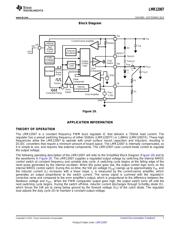
In the Simplifed Block Diagram of Figure 19, capacitor C
BOOST
and diode D2 supply the gate-drive current for the
NMOS switch. Capacitor C
BOOST
is charged via diode D2 by V
IN
. During a normal switching cycle, when the
internal NMOS control switch is off (T
OFF
) (refer to Figure 20), V
BOOST
equals V
IN
minus the forward voltage of D2
(V
FD2
), during which the current in the inductor (L) forward biases the Schottky diode D1 (V
FD1
). Therefore the
voltage stored across C
BOOST
is
V
BOOST
- V
SW
= V
IN
- V
FD2
+ V
FD1
(1)
8 Submit Documentation Feedback Copyright © 2013, Texas Instruments Incorporated
Product Folder Links: LMR12007
器件 Datasheet 文档搜索
AiEMA 数据库涵盖高达 72,405,303 个元件的数据手册,每天更新 5,000 多个 PDF 文件
