Datasheet 搜索 > TI(德州仪器) > LP2950-30 数据手册 > LP2950-30 数据手册 17/32 页

¥ 0
LP2950-30 数据手册 - TI(德州仪器)
制造商:
TI(德州仪器)
封装:
TO-92-3
Pictures:
3D模型
符号图
焊盘图
引脚图
产品图
页面导航:
引脚图在P3Hot
典型应用电路图在P16P17P18
原理图在P12P13
封装尺寸在P20P21P23P24
标记信息在P20P21
封装信息在P19P20P21P22P23P24
技术参数、封装参数在P4P5
应用领域在P1P32
电气规格在P5P6
导航目录
LP2950-30数据手册
Page:
of 32 Go
若手册格式错乱,请下载阅览PDF原文件

® =
p ´ ´
;
(CBYPASS) (BYPASS)
1
f 200 Hz C
2 R1 200 Hz
LP2950
,
LP2951
www.ti.com
SLVS582I –APRIL 2006–REVISED NOVEMBER 2014
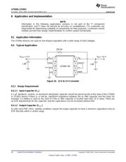
Typical Application (continued)
8.2.2 Detailed Design Procedure
8.2.2.1 Capacitance Value
For V
OUT
≥ 5 V, a minimum of 1 μF is required. For lower V
OUT
, the regulator’s loop gain is running closer to unity
gain and, thus, has lower phase margins. Consequently, a larger capacitance is needed for stability.
For V
OUT
= 3 V or 3.3 V, a minimum of 2.2 μF is recommended. For worst case, V
OUT
= 1.23 V (using the ADJ
version), a minimum of 3.3 μF is recommended. C
OUT
can be increased without limit and only improves the
regulator stability and transient response. Regardless of its value, the output capacitor should have a resonant
frequency greater than 500 kHz.
The minimum capacitance values given above are for maximum load current of 100 mA. If the maximum
expected load current is less than 100 mA, then lower values of C
OUT
can be used. For instance, if I
OUT
< 10 mA,
then only 0.33 μF is required for C
OUT
. For I
OUT
< 1 mA, 0.1 μF is sufficient for stability requirements. Thus, for a
worst-case condition of 100-mA load and V
OUT
= V
REF
= 1.235 V (representing the highest load current and
lowest loop gain), a minimum C
OUT
of 3.3 μF is recommended.
For the LP2950/51, no load stability is inherent in the design — a desirable feature in CMOS circuits that are put
in standby (such as RAM keep-alive applications). If the LP2951 is used with external resistors to set the output
voltage, a minimum load current of 1 μA is recommended through the resistor divider.
8.2.2.2 Capacitor Types
Most tantalum or aluminum electrolytics are suitable for use at the input. Film-type capacitors also work but at
higher cost. When operating at low temperature, care should be taken with aluminum electrolytics, as their
electrolytes often freeze at –30°C. For this reason, solid tantalum capacitors should be used at temperatures
below –25°C.
Ceramic capacitors can be used, but due to their low ESR (as low as 5 mΩ to 10 mΩ), they may not meet the
minimum ESR requirement previously discussed. If a ceramic capacitor is used, a series resistor between
0.1 Ω to 2 Ω must be added to meet the minimum ESR requirement. In addition, ceramic capacitors have one
glaring disadvantage that must be taken into account — a poor temperature coefficient, where the capacitance
can vary significantly with temperature. For instance, a large-value ceramic capacitor (≥ 2.2 μF) can lose more
than half of its capacitance as temperature rises from 25°C to 85°C. Thus, a 2.2-μF capacitor at 25°C drops well
below the minimum C
OUT
required for stability as ambient temperature rises. For this reason, select an output
capacitor that maintains the minimum 2.2 μF required for stability for the entire operating temperature range.
8.2.2.3 C
BYPASS
: Noise and Stability Improvement
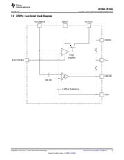
In the LP2951 device, an external FEEDBACK pin directly connected to the error amplifier noninverting input can
allow stray capacitance to cause instability by shunting the error amplifier feedback to GND, especially at high
frequencies. This is worsened if high-value external resistors are used to set the output voltage, because a high
resistance allows the stray capacitance to play a more significant role; i.e., a larger RC time delay is introduced
between the output of the error amplifier and its FEEDBACK input, leading to more phase shift and lower phase
margin. A solution is to add a 100-pF bypass capacitor (C
BYPASS
) between OUTPUT and FEEDBACK; because
C
BYPASS
is in parallel with R1, it lowers the impedance seen at FEEDBACK at high frequencies, in effect
offsetting the effect of the parasitic capacitance by providing more feedback at higher frequencies. More
feedback forces the error amplifier to work at a lower loop gain, so C
OUT
should be increased to a minimum of
3.3 μF to improve the regulator’s phase margin.
C
BYPASS
can be also used to reduce output noise in the LP2951 device. This bypass capacitor reduces the
closed loop gain of the error amplifier at the high frequency, so noise no longer scales with the output voltage.
This improvement is more noticeable with higher output voltages, where loop gain reduction is greatest. A
suitable C
BYPASS
is calculated as shown in Equation 2:
(2)
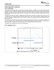
On the 3-pin LP2950 device, noise reduction can be achieved by increasing the output capacitor, which causes
the regulator bandwidth to be reduced, thus eliminating high-frequency noise. However, this method is relatively
inefficient, as increasing C
OUT
from 1 μF to 220 μF only reduces the regulator’s output noise from
430 μV to 160 μV (over a 100-kHz bandwidth).
Copyright © 2006–2014, Texas Instruments Incorporated Submit Documentation Feedback 17
Product Folder Links: LP2950 LP2951
器件 Datasheet 文档搜索
AiEMA 数据库涵盖高达 72,405,303 个元件的数据手册,每天更新 5,000 多个 PDF 文件
