Datasheet 搜索 > 比较器 > TI(德州仪器) > LP339N/NOPB 数据手册 > LP339N/NOPB 数据手册 5/14 页
 器件3D模型
¥ 9.194
LP339N/NOPB 数据手册 - TI(德州仪器)
制造商:
TI(德州仪器)
分类:
比较器
封装:
PDIP-14
描述:
LP 系列低功耗比较器### 比较器,Texas InstrumentsTexas Instruments 系列电压比较器不仅包括传统单、双和四路比较器封装,还包括窗口比较器及过压和欠压监控器。 尽管比较器和运算放大器表面上是相似的设备,但它们在实用应用中的操作大大不同。 运算放大器适用于线性操作,附带适当反馈,而比较器定制用于快速切换且通常在开路模式中操作。 专用电压比较器具有明显较短的传播延迟,且可在饱和条件下具有更快的响应时间。 大多数比较器还更耐受高差分输入电压,且很多比较器具有开路集电极输出,从而可与其他设备并联操作。
Pictures:
3D模型
符号图
焊盘图
引脚图
产品图
页面导航:
导航目录
LP339N/NOPB数据手册
Page:
of 14 Go
若手册格式错乱,请下载阅览PDF原文件
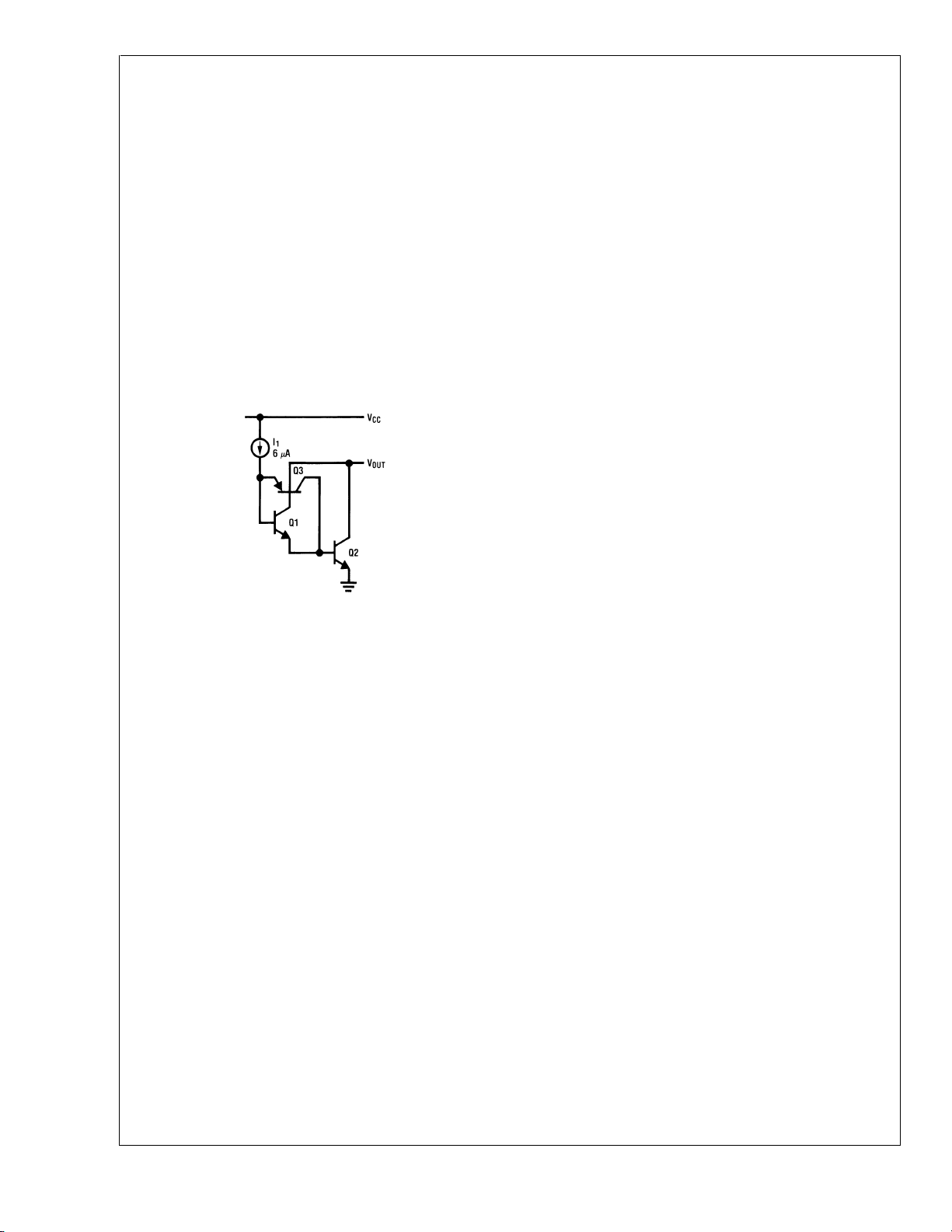
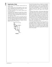
Application Hints
All pins of any unused comparators should be tied to the
negative supply.
The bias network of the LP339 establishes a drain current
which is independent of the magnitude of the power supply
voltage over the range of from 2 V
DC
to 30 V
DC
.
It is usually unnecessary to use a bypass capacitor across
the power supply line.
The differential input voltage may be larger than V+ without
damaging the device. Protection should be provided to pre-
vent the input voltages from going negative more than −0.3
V
DC
(at 25˚C). An input clamp diode can be used as shown
in the application section.
The output section of the LP339 has two distinct modes of
operation-a Darlington mode and a grounded emitter mode.
This unique drive circuit permits the LP339 to sink 30 mA at
V
O
=2 V
DC
(Darlington mode) and 700 µA at V
O
=0.4 V
DC
(grounded emitter mode).
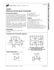
Figure 1
is a simplified schematic
diagram of the LP339 output section.
Notice that the output section is configured in a Darlington
connection (ignoring Q3). Therefore, if the output voltage is
held high enough (V
O
≥1V
DC
), Q1 is not saturated and the
output current is limited only by the product of the betas of
Q1, Q2 and I1 (and the 60Ω R
SAT
of Q2). The LP339 is thus
capable of driving LED’s, relays, etc. in this mode while
maintaining an ultra-low power supply current of typically
60 µA.
If transistor Q3 were omitted, and the output voltage allowed
to drop below about 0.8 V
DC
, transistor Q1 would saturate
and the output current would drop to zero. The circuit would,
therefore, be unable to “pull” low current loads down to
ground (or the negative supply, if used). Transistor Q3 has
been included to bypass transistor Q1 under these condi-
tions and apply the current I1 directly to the base of Q2. The
output sink current is now approximately I1 times the beta of
Q2 (700 µA at V
O
=0.4 V
DC
). The output of the LP339 exhib-
its a bi-modal characteristic with a smooth transition be-
tween modes. (See Output Sink Current graphs in Typical
Performance Characteristics section.)
It is also important to note that in both cases the output is an
uncommitted collector. Therefore, many collectors can be
tied together to provide an output OR’ing function. An output
pull-up resistor can be connected to any available power
supply voltage within the permitted power supply voltage
range and there is no restriction on this voltage due to the
magnitude of the voltage which is applied to the V+ terminal
of the LP339 package.
DS005226-11
FIGURE 1.
LP339
www.national.com 4
器件 Datasheet 文档搜索
AiEMA 数据库涵盖高达 72,405,303 个元件的数据手册,每天更新 5,000 多个 PDF 文件
